Supercharge Your Innovation With Domain-Expert AI Agents!

Method for manufacturing rear side local contact silicon solar cell

A silicon solar cell, local contact technology, applied in the final product manufacturing, sustainable manufacturing/processing, circuits, etc., can solve the problems of silicon wafer pollution, difficult to burn through the passivation layer, difficult ohmic contact, etc., and achieve the goal of reducing damage Effect

Active Publication Date: 2013-10-23
WUXI SUNTECH POWER CO LTD
View PDF8 Cites 4 Cited by
  • Summary
  • Abstract
  • Description
  • Claims
  • Application Information

AI Technical Summary

Problems solved by technology

[0006] The above-mentioned method of corroding a local area of ​​the passivation layer with a corrosive slurry to make a local contact has the problems that the manufacturing process is complicated and it is difficult to form a good ohmic contact between the local contact and the silicon wafer due to reasons such as poor corrosion; and The above-mentioned method of printing paste directly on the local area of ​​the passivation layer on the back of the silicon wafer and sintering to form a local contact is also difficult to form a good ohmic contact because it is difficult to accurately burn through the passivation layer
[0007] In order to solve the above-mentioned problem that it is difficult to form a good ohmic contact between the local contact and the silicon wafer, the existing technology also forms a local contact on the local area of ​​the back of the silicon wafer by means of screen printing before forming a passivation layer on the back, Then through sintering, the local contact is heavily doped into the silicon wafer to form a heavily doped back field, and then a passivation layer is formed
This method can form a good ohmic contact between the silicon wafer and the back contact, but there is no passivation layer on the back of the silicon wafer during the sintering process, and the high temperature of sintering is likely to cause the silicon wafer to be contaminated by impurities, thereby reducing the electrical capacity of the silicon solar cell. performance

Method used


Image

  • Method for manufacturing rear side local contact silicon solar cell

Examples


Embodiment Construction

[0020] specific implementation plan

[0021] The purpose and effects of the present invention will be described in detail below in conjunction with specific embodiments and accompanying drawings.

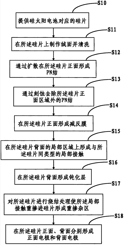
[0022] see figure 1 , the method for manufacturing a silicon solar cell with backside partial contact firstly proceeds to step S10 to provide a silicon wafer corresponding to the silicon solar cell. In this embodiment, the silicon wafer is a P-type single crystal silicon wafer, its resistivity is 0.5˜10 Ω·cm, its thickness is 200 μm˜400 μm, and its size is 125 mm×125 mm.

[0023] Then continue to step S11, making a textured surface on the silicon wafer and cleaning it, adopting different texturing methods for single crystal silicon wafers and polycrystalline silicon wafers, and using alkaline solutions such as potassium hydroxide or sodium hydroxide for single crystal silicon wafers Form a pyramid-like suede surface on the silicon wafer. When it is a polycrystalline silicon wafer,...


PUM

PropertyMeasurementUnit
Resistivityaaaaaaaaaa
Thicknessaaaaaaaaaa

Abstract

The invention provides a method for manufacturing a rear side local contact silicon solar cell. In the prior art, local contact and a silicon wafer cannot form good ohmic contact, or the electrical performance of the silicon wafer, which is provided with local contact but no passivation layer at the rear side, is reduced because of heat treatment is carried out on the silicon wafer. The method provided by the invention comprises the steps of: firstly, texturing and cleaning a corresponding silicon wafer of the silicon solar cell, forming a PN junction at the front side of the silicon wafer through diffusion, thereafter removing the PN junction outside a front side region of the silicon wafer through etching, then forming an antireflection film at the front side of the silicon wafer and forming the same type of local contact as the silicon wafer in the local region of the rear side, thereafter forming a passivation layer at the rear side, then sintering the silicon wafer so as to enable the local contact to be heavily doped into the silicon wafer to form a heavily doped region, and finally forming a front side electrode and a rear side electrode at the front side and the rear side of the silicon wafer respectively. The method provided by the invention can improve the ohmic contact between the local contact and the silicon wafer, and can reduce damages produced by heat treatment in the absent of the passivation layer.

Description

technical field [0001] The invention relates to a silicon solar cell manufacturing process, in particular to a method for manufacturing a silicon solar cell with partial back contact. Background technique [0002] A silicon solar cell is essentially a PN junction device. The photo-generated carriers generated by light are driven to both sides of the PN junction through the electric field of the PN junction to form a photo-generated current, thereby achieving the effect of photoelectric conversion. In order to reduce the recombination of photogenerated carriers and improve the electrical performance of silicon solar cells, structures or measures to reduce the recombination mechanism are added in the silicon wafer body and surface. In the body, high-purity, low-defect, low-oxygen silicon single crystal or polycrystalline materials should be selected; on the back, the back electric field is formed by heavily doping the same type of material as the silicon wafer, and the drift s...

Claims


Application Information

Patent Timeline
IPC IPC(8): H01L31/18H01L31/0224
CPCY02P70/50
Inventor 孟庆蕾陆红艳蒋林华姜勇飞黄铖王振交韩培育吴甲奇钱洪强
Owner WUXI SUNTECH POWER CO LTD
Features
  • R&D
  • Intellectual Property
  • Life Sciences
  • Materials
  • Tech Scout
  • Unparalleled Data Quality
  • Higher Quality Content
  • 60% Fewer Hallucinations
Learn More