Gallium nitride substrate and epitaxial wafer

一种氮化镓基板、物理性的技术,应用在半导体器件、电气元件、半导体/固态器件制造等方向,能够解决不良、发光强度降低、成品率降低等问题

Inactive Publication Date: 2013-10-23
SUMITOMO CHEM CO LTD
View PDF13 Cites 5 Cited by
  • Summary
  • Abstract
  • Description
  • Claims
  • Application Information

AI Technical Summary

Problems solved by technology

In the case of manufacturing an optical device using such an epitaxial wafer, there arises a problem that a defect due to a decrease in luminous intensity occurs and the yield decreases.

Method used


Image

  • Gallium nitride substrate and epitaxial wafer
  • Gallium nitride substrate and epitaxial wafer
  • Gallium nitride substrate and epitaxial wafer

Examples


Embodiment approach

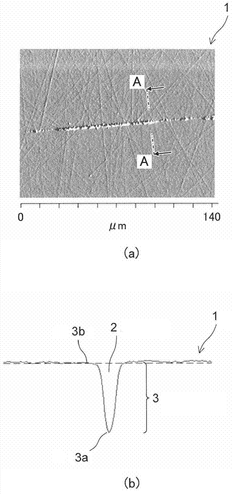
[0037] The inventors of the present invention conducted in-depth investigations and found that even if there is a physical level difference caused by scratches on the surface of the gallium nitride substrate, it is not necessarily impossible to achieve good epitaxial crystal growth. The size of the physical height difference is relatively small, and the difference in the intensity of cathodoluminescence at the wavelength corresponding to the band gap of the gallium nitride substrate at the upper and lower parts of the physical height difference is small, and the abnormality of the crystal on the substrate can be suppressed Growth can grow crystals with flat surfaces.

[0038] The intensity of cathodoluminescence varies depending on the state of the crystals at the measurement site, and if the difference in the intensity of cathodoluminescence between the upper and lower parts of the physical level difference is large, it means that the crystal states of the upper and lower part...

Embodiment 1

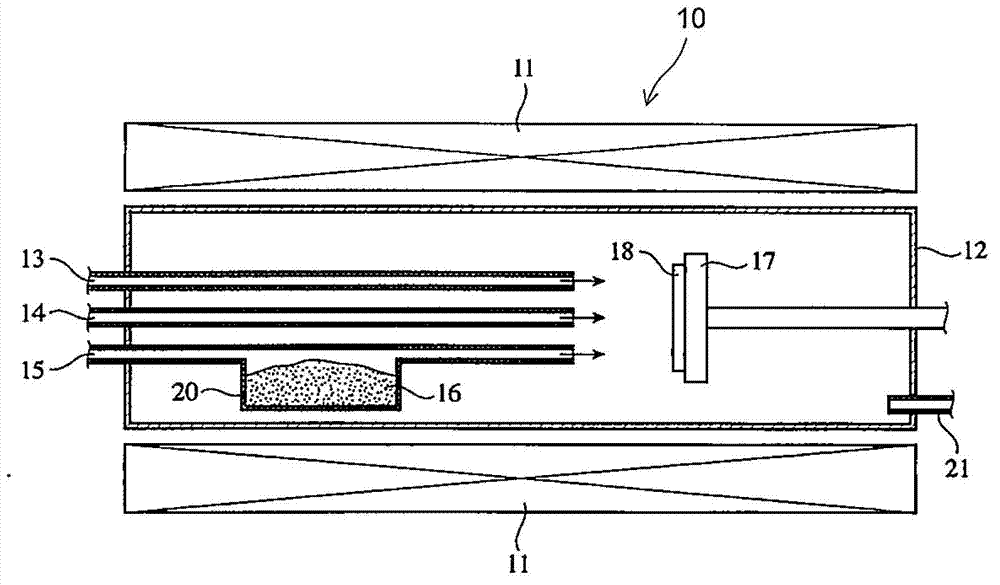
[0063] In Example 1, 25 gallium nitride substrates were formed by the VAS method. Next, the physical height difference was measured for each substrate using a three-dimensional optical profiler, and 20 evaluation regions were determined for the size of the physical height difference. Next, cathodoluminescence measurement was performed on each evaluation region of each substrate. Next, an epitaxial growth layer was grown on each gallium nitride substrate to form a quantum well structure, and an epitaxial wafer was obtained. Next, photoluminescence measurement was performed on each epitaxial wafer, and the average measurement value in each evaluation area was obtained to evaluate the surface flatness, and the relationship between the size of the physical height difference and the result of cathodoluminescence measurement was investigated. The specific steps are described below.

[0064] (Manufacturing of gallium nitride substrates)

[0065] First, a GaN base layer with a thic...

Embodiment 2

[0111] In Example 2, the implementation conditions of the mechanical polishing of the Ga polar surface in the manufacturing steps of the gallium nitride substrates (1) to (25) in Example 1 were respectively changed to pressure: 0.45 MPa and polishing implementation time: In 25 minutes, gallium nitride substrates ( 26 ) to ( 50 ) were produced. Other manufacturing conditions are the same as those of gallium nitride substrates (1) to (25).

[0112] (Measurement of physical height difference)

[0113] By the same method as in Example 1, the physical height differences caused by scratches and the like on the surfaces of the gallium nitride substrates (26) to (50) were measured, and 10 evaluation regions d1 were determined for the size of the physical height differences. ~d10.

[0114] In the gallium nitride substrates ( 26 ) to ( 50 ), no physical difference in height exceeding 2 μm was observed. This is considered to be because the surface of the substrate was further flattene...


PUM

PropertyMeasurementUnit
diameteraaaaaaaaaa
wavelengthaaaaaaaaaa

Abstract

The invention provides a gallium nitride substrate that is capable of growing an epitaxial growth layer having a good crystalline quality even if the surface has physical level differences, and an epitaxial wafer that a surface thereof has good flatness by growing the epitaxial growth layer on the above-mentioned gallium nitride substrate. According to one embodiment of the invention, the gallium nitride substrate (1) comprises: a plurality of physical level differences (3) in a surface thereof. All the physical level differences (3) existing in the surface have a dimension of not more than 4 mum. A relationship of (H-L) / H100<=80 is satisfied in all the physical level differences (3), where H represents a higher value of cathodoluminescence emission intensities of a wavelength corresponding to a bandgap of the gallium nitride substrate, and L represents a lower value of the cathodoluminescence emission intensities, the cathodoluminescence emission intensities being measured in an upper step (3b) and a lower step (3a) of the physical level difference.

Description

technical field [0001] The invention relates to a gallium nitride substrate and an epitaxial wafer. Background technique [0002] As a method of manufacturing a good-quality and large-scale gallium nitride substrate, the following methods are known: Dislocation Elimination by the Epi-growth with Inverted-Pyramidal Pits : For example, refer to the patent document 1) method, VAS method (pore-assisted separation method, Void-Assisted Separation Method: for example, refer to the patent document 2) to obtain a gallium nitride substrate method, by HVPE (Hydride Vapor Phase Epitaxy, Hydride Vapor Phase Epitaxy ) method to grow a gallium nitride single crystal thickly on a different kind of substrate, and peel it off from the different kind of substrate to obtain a gallium nitride self-supporting substrate. [0003] In gallium nitride substrates produced by these methods, the dislocation density changes in the thickness direction from the back surface toward the surface, and the la...

Claims


Application Information

Patent Timeline
Patent Type & Authority Applications(China)
IPC IPC(8): H01L33/02
CPCY10S438/962H01L21/02505H01L21/0254H01L29/2003H01L21/02389H01L21/02458H01L21/0262
Inventor 山本俊辅
Owner SUMITOMO CHEM CO LTD
Why Eureka
Try Eureka