Gate structure and forming method thereof, semiconductor structure and forming method thereof

A gate structure and semiconductor technology, applied in semiconductor devices, semiconductor/solid-state device manufacturing, electrical components, etc., can solve problems such as increased leakage current of MOS transistors, reduced reliability of gate oxide layers, and damage to gate oxide layers and polysilicon gates. , to reduce the gate leakage current

Active Publication Date: 2013-10-30
SEMICON MFG INT (SHANGHAI) CORP
View PDF5 Cites 7 Cited by
  • Summary
  • Abstract
  • Description
  • Claims
  • Application Information

AI Technical Summary

Problems solved by technology

[0003] However, in the process of dry etching the polysilicon layer and the silicon oxide layer to form the gate oxide layer and the polysilicon gate, the dry etching process will cause damage to the gate oxide layer and the polysilicon gate, so that the gate oxide layer and the polysilicon gate Gate sidewalls can generate many defects
The defects will affect the integrity of the gate oxide layer, which will easily reduce the reliability of the gate oxide layer and reduce the breakdown voltage of the gate oxide layer. At the same time, the defects will also easily increase the leakage current of the MOS transistor.

Method used


Image

  • Gate structure and forming method thereof, semiconductor structure and forming method thereof
  • Gate structure and forming method thereof, semiconductor structure and forming method thereof
  • Gate structure and forming method thereof, semiconductor structure and forming method thereof

Examples


Embodiment Construction

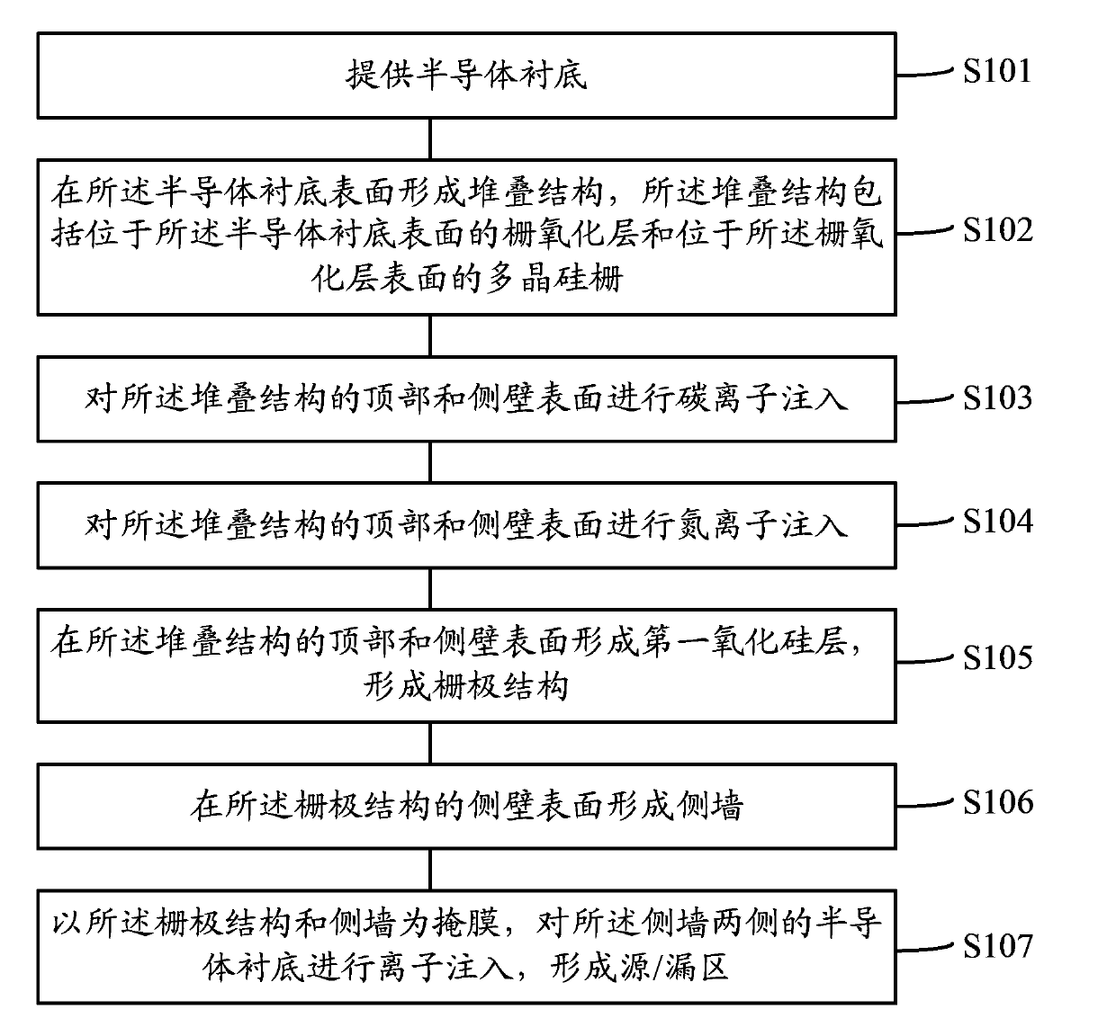
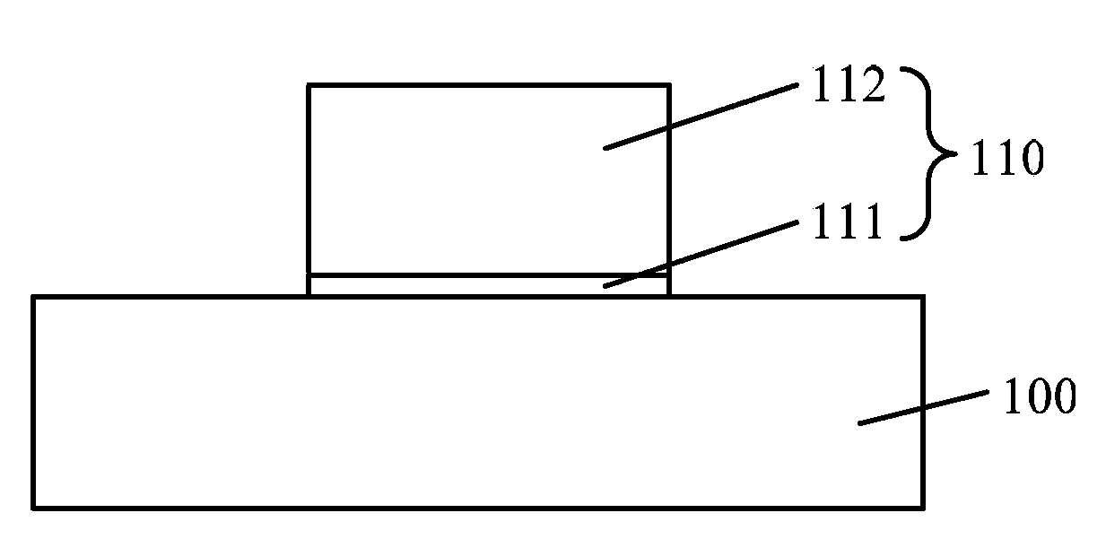
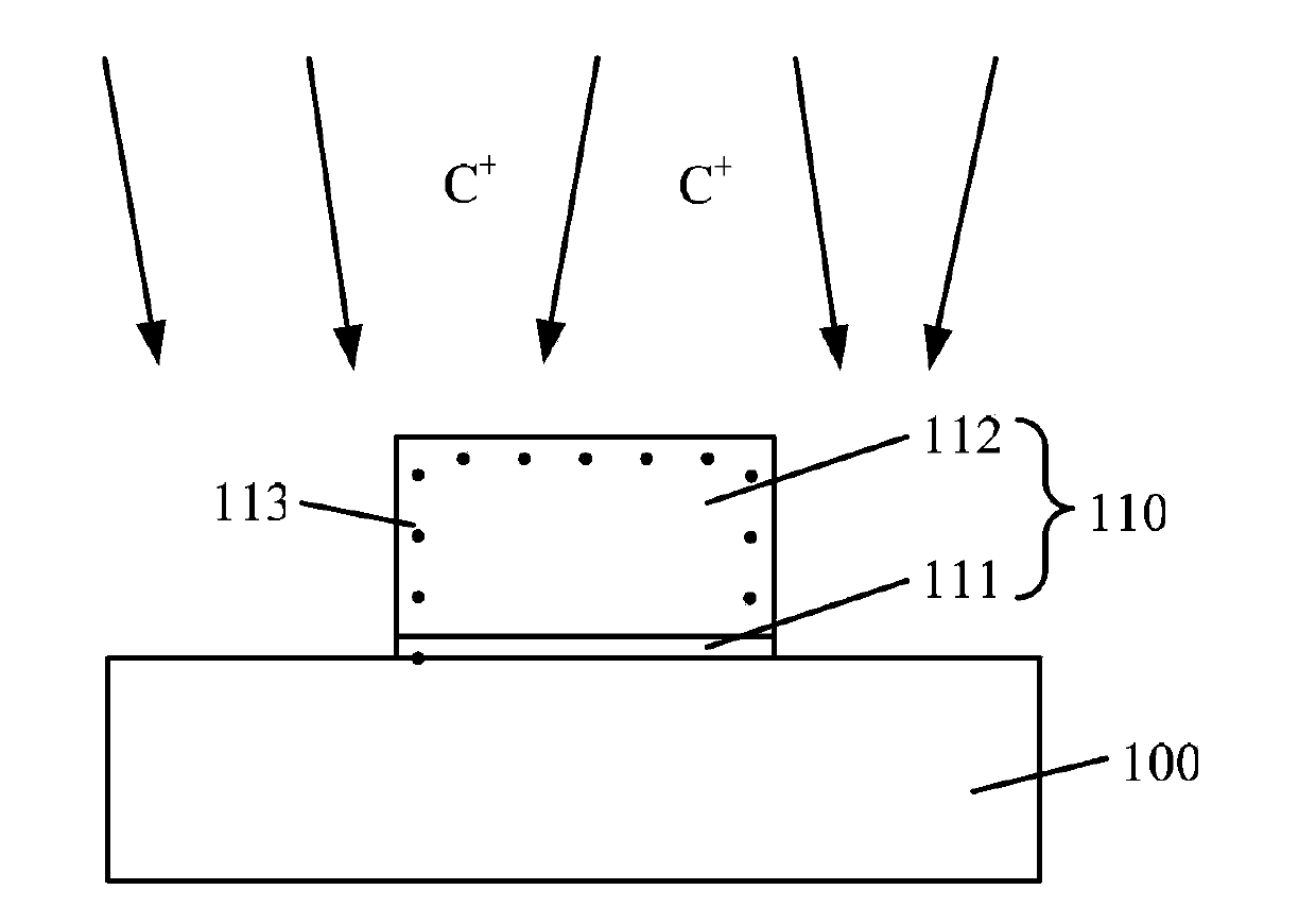
[0061] The inventor has found through research that in the prior art, as the operating frequency requirements of semiconductor devices are getting faster and the power consumption requirements are getting lower and lower, the polysilicon gates are usually doped with impurity ions, and the impurity ions are usually Boron ions or phosphorus ions are used to increase the mobility of carriers and reduce the resistance of the polysilicon gate. However, when the re-oxidation process forms a silicon oxide layer on the top and sidewall surfaces of the polysilicon gate structure, due to the strong mobility of boron ions or phosphorous ions, oxidation-enhanced diffusion (Oxidation Enhanced Diffusion, OED) Under the action of the boron ions or phosphorous ions, it is easy to diffuse to the silicon oxide layer and the gate oxide layer, so that the boron ions or phosphorous ions in the polysilicon gate near the silicon oxide layer and the gate oxide layer diffuse toward the oxide layer Dif...


PUM


Abstract

The invention discloses a gate structure, a forming method of the gate structure, a semiconductor structure with the gate structure and a forming method of the semiconductor structure. The forming method of the gate structure comprises the steps that a semiconductor substrate is provided; a stack structure is formed on the surface of the semiconductor substrate, wherein the stack structure comprises a gate oxide layer located on the surface of the semiconductor substrate and polysilicon gate located on the surface of the gate oxide layer; carbon ion implantation is conducted on the top of the stack structure and the surface of the side wall of the stack structure; nitrogen ion implantation is conducted on the top of the stack structure and the surface of the side wall of the stack structure; first monox layers are formed on the top of the stack structure and the surface of the side wall of the stack structure. Due to the fact that nitrogen ions and carbon ions implanted into the polysilicon gate can serve as impurity traps, the enhanced diffusion effect of foreign ions, close to the surface, of the polysilicon gate is restrained, the dosage concentration of the foreign ions, close to the surface, of the polysilicon gate and the dosage concentration of foreign ions inside the polysilicon gate are the same almost, and the resistance of the polysilicon gate will not improved.

Description

technical field [0001] The present invention relates to the field of semiconductors, in particular to a gate structure and a forming method, a semiconductor structure having the gate structure and a forming method. Background technique [0002] Polysilicon gate structures are often used in the fabrication of metal oxide semiconductor (MOS) transistors. In a typical polysilicon gate structure formation process, a silicon oxide layer is first formed on the surface of the semiconductor substrate, a polysilicon layer is formed on the surface of the silicon oxide layer, and a patterned photoresist is formed on the surface of the polysilicon layer by photolithography. Layer, using the patterned photoresist layer as a mask, dry-etching the polysilicon layer and the silicon oxide layer in sequence to form a polysilicon gate structure on the surface of the semiconductor substrate, and the polysilicon gate The structure includes a gate oxide layer on the surface of the semiconductor ...

Claims


Application Information

Patent Timeline
Patent Type & Authority Applications(China)
IPC IPC(8): H01L29/423H01L21/28H01L29/78H01L21/336H01L21/265
Inventor 赵猛
Owner SEMICON MFG INT (SHANGHAI) CORP
Why Eureka
Try Eureka