Reverse conducting insulated gate bipolar transistor (RC-IGBT) device

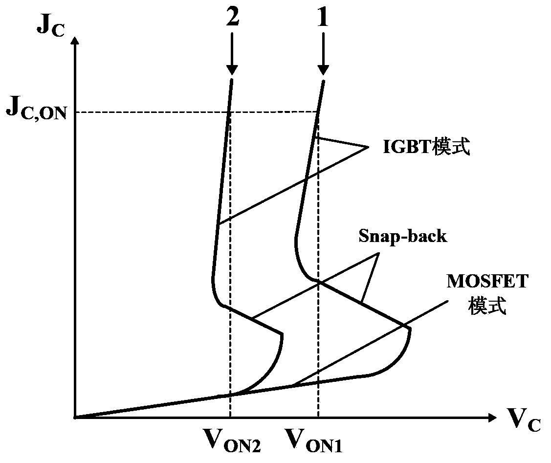
A reverse conduction device technology, applied in the field of power semiconductor devices, can solve the problems of increasing the forward conduction voltage drop of the IGBT, reducing the injection efficiency of the P+ collector region 10, and weakening the conductance modulation effect.

Inactive Publication Date: 2013-11-06
UNIV OF ELECTRONICS SCI & TECH OF CHINA +1
View PDF4 Cites 12 Cited by
  • Summary
  • Abstract
  • Description
  • Claims
  • Application Information

AI Technical Summary

Problems solved by technology

Reducing the doping concentration of the P+ collector region 10 or using a narrow bandgap semiconductor can reduce the built-in potential, but this will greatly reduce the injection efficiency of the P+ collector region 10 into the N-drift region 7, weakening the conductance modulation effect, Increase the forward conduction voltage drop of the IGBT

Method used


Image

  • Reverse conducting insulated gate bipolar transistor (RC-IGBT) device
  • Reverse conducting insulated gate bipolar transistor (RC-IGBT) device
  • Reverse conducting insulated gate bipolar transistor (RC-IGBT) device

Examples


Embodiment Construction

[0026] The RC-IGBT device provided by the present invention will be further described below by taking the first conductivity type semiconductor material as a P-type semiconductor material and the second conductivity type semiconductor material as an N-type semiconductor material as an example.

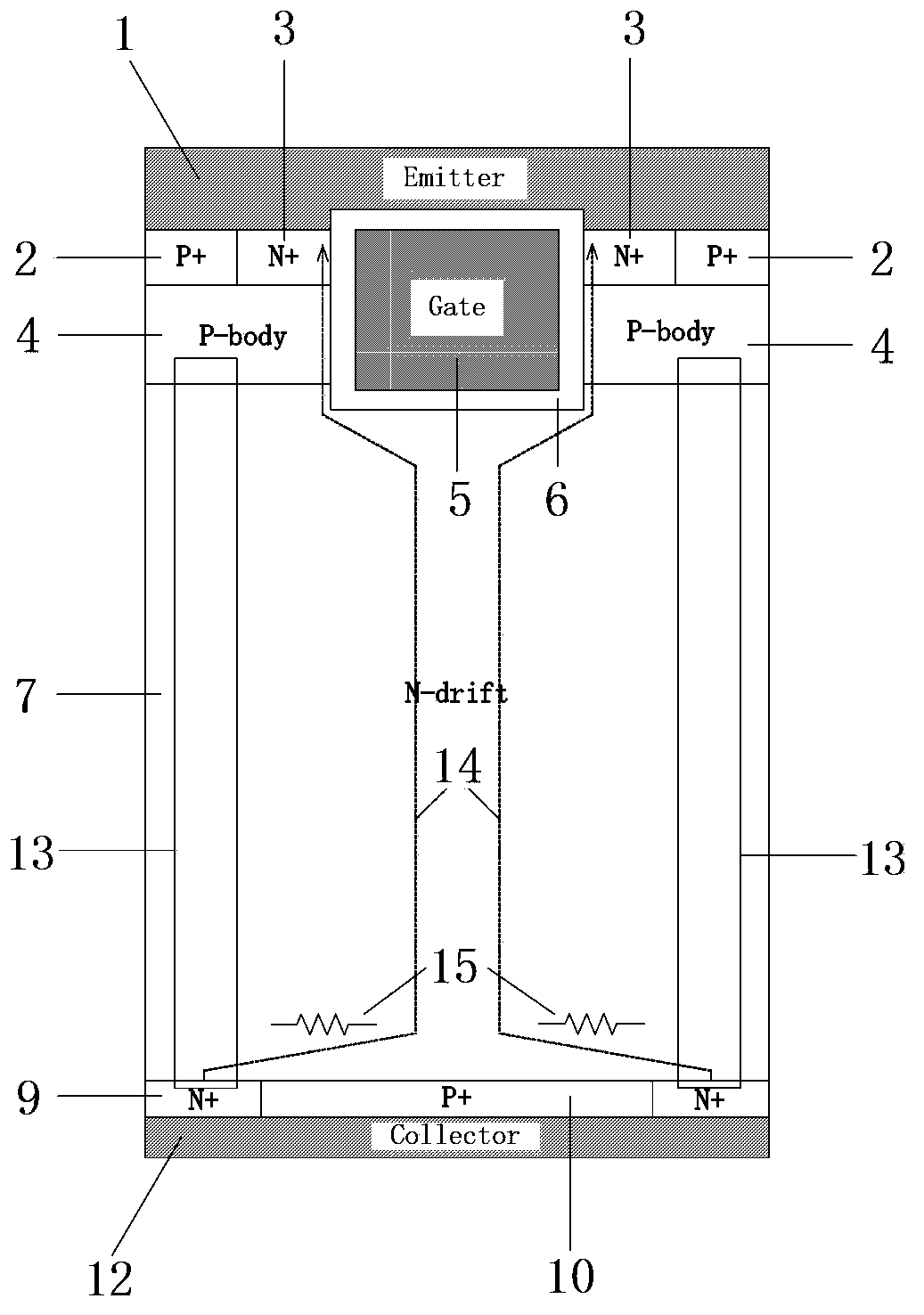
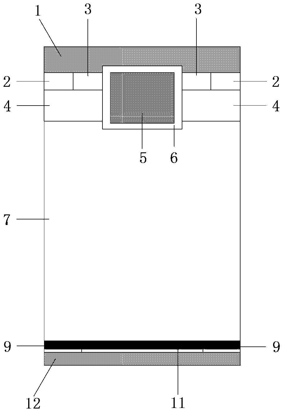
[0027] A reverse conduction type IGBT device, its structure is as follows Figure 5 As shown, it includes an emitter structure, a collector structure, a gate structure and a drift region structure; the emitter structure includes a metal emitter 1, a P+ ohmic contact region 2, an N+ emitter region 3 and a P-type body region 4, wherein P+ The ohmic contact region 2 and the N+ emitter region 3 are independently located in the P-type body region 4, and the surfaces of the P+ ohmic contact region 2 and the N+ emitter region 3 are all in contact with the metal emitter 1; the collector structure includes a P+ collector Electric region 11, N+ collector short-circuit region 9 and metal collecto...


PUM


Abstract

The invention relates to an RC-IGBT device and belongs to the technical field of power semi-conductor devices. Variable-component mixed crystals are used for producing a collector region of the IGBT to form an energy band structure with gradually variable forbidden bandwidth. The forbidden bandwidth is small at the junction of the collector region and a drift region, built-in electrical potentials of the collector region and the drift region are reduced, and the phenomenon of snap-back is relieved; meanwhile, the gradually variable forbidden bandwidth is formed due to the variable-component materials of the collector region, and a retarding field of minority carriers is generated in the collector region, so that injection of the minority carriers to the collector region by the drift region is reduced, the injection efficiency of the collector region to the drift region is improved, the strong conductivity modulation effect can be obtained, and the forward conducting voltage drop of the IGBT is reduced.

Description

technical field [0001] The invention belongs to the technical field of power semiconductor devices, and in particular relates to a reverse conduction type insulated gate bipolar transistor (IGBT) for alleviating the snap-back phenomenon. technical background [0002] IGBT is the most representative device in the current medium and high power power system. It combines the advantages of easy driving of MOSFET, simple control, high switching frequency and low conduction voltage of power transistor, and is widely used in civil, commercial, national defense and other fields. [0003] When IGBTs are used as switching elements to handle high-power signals, each IGBT needs to be equipped with an anti-parallel diode with the same withstand voltage for freewheeling. Therefore, usually IGBT manufacturers will also design corresponding IGBTs when designing and manufacturing IGBTs. Freewheeling diode; At present, in most products, this diode needs to be manufactured separately on anothe...

Claims


Application Information

Patent Timeline
Patent Type & Authority Applications(China)
IPC IPC(8): H01L29/739H01L29/06
Inventor 任敏宋询奕李果顾鸿鸣张鹏吴明进曾智李泽宏张金平张波
Owner UNIV OF ELECTRONICS SCI & TECH OF CHINA
Why Eureka
Try Eureka