A reverse conduction igbt device
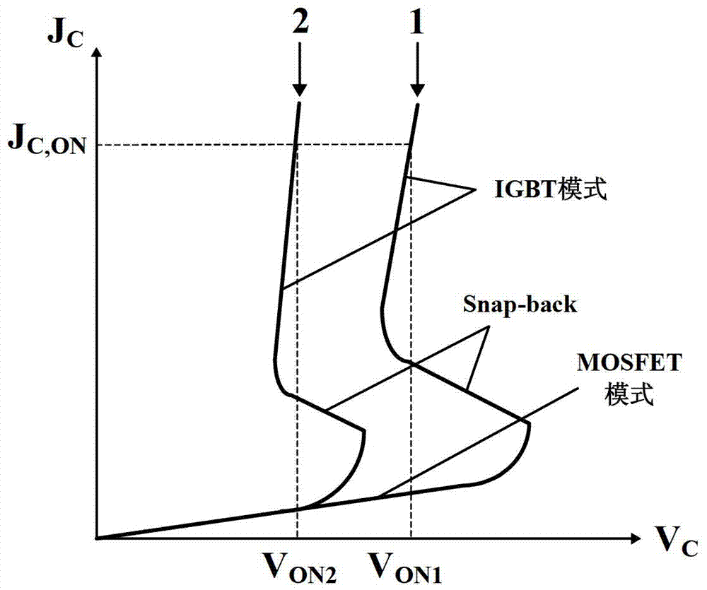
A reverse conduction device technology, applied in the field of power semiconductor devices, can solve the problems of increasing the IGBT forward conduction voltage drop, reducing the injection efficiency of the P+ collector region 10, and weakening the conductance modulation effect.
- Summary
- Abstract
- Description
- Claims
- Application Information
AI Technical Summary
Problems solved by technology
Method used
Image
Examples
Embodiment Construction
[0026] The RC-IGBT device provided by the present invention will be further described below by taking the first conductivity type semiconductor material as a P-type semiconductor material and the second conductivity type semiconductor material as an N-type semiconductor material as an example.
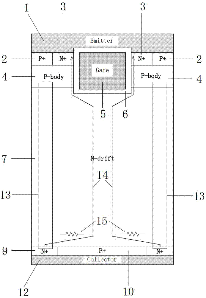
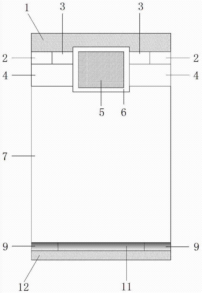
[0027] A reverse conduction type IGBT device, its structure is as follows Figure 5 As shown, it includes an emitter structure, a collector structure, a gate structure and a drift region structure; the emitter structure includes a metal emitter 1, a P+ ohmic contact region 2, an N+ emitter region 3 and a P-type body region 4, wherein P+ The ohmic contact region 2 and the N+ emitter region 3 are independently located in the P-type body region 4, and the surfaces of the P+ ohmic contact region 2 and the N+ emitter region 3 are all in contact with the metal emitter 1; the collector structure includes a P+ collector Electric region 11, N+ collector short-circuit region 9 and metal collecto...
PUM
 Abstract
Description
Claims
Application Information


