Gallium nitride power field effect transistor

A power field effect and gallium nitride technology, which is applied in semiconductor devices, electrical components, circuits, etc., can solve problems such as incompatibility, poor repeatability and reliability, and increased GaN field effect transistor process steps, so as to increase the turn-on voltage, Effects of improving switching performance and reducing power loss

Inactive Publication Date: 2013-11-13
无锡派腾微纳米科技有限公司
View PDF2 Cites 4 Cited by
  • Summary
  • Abstract
  • Description
  • Claims
  • Application Information

AI Technical Summary

Problems solved by technology

Using the above method will increase the process steps of making GaN field effect transistors, and there are still technical problems of poor repeatability and reliability, and some of the process flows are not compatible with standard process flows, which increases the difficulty of implementation

Method used


Image

  • Gallium nitride power field effect transistor
  • Gallium nitride power field effect transistor
  • Gallium nitride power field effect transistor

Examples


Embodiment Construction

[0022] In order to make the above objects, features and advantages of the present invention more comprehensible, specific implementations of the present invention will be described in detail below in conjunction with the accompanying drawings and embodiments.

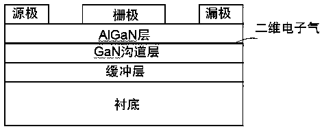
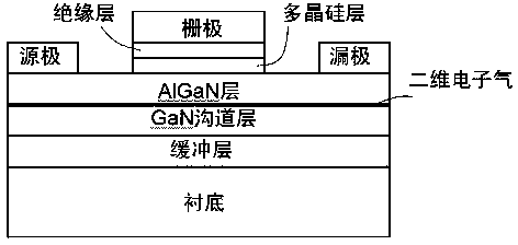
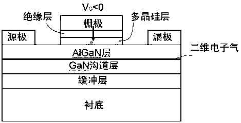
[0023] figure 2 is a schematic cross-sectional view of a GaN field effect transistor provided by an embodiment of the present invention.

[0024] In this embodiment, the substrate adopts single crystal silicon with a thickness of 300 micrometers; the material of the buffer layer is aluminum nitride, and the thickness of the buffer layer is 10 nanometers; the thickness of the GaN channel layer is 2 micrometers; the thickness of the AlGaN layer is 20 nanometers. nm; the metal layer structure of the source and drain is Ti / Al / Ni / Au; the thickness of the polysilicon layer is 1 nm; the material of the insulating layer is aluminum oxide, and the thickness is 0.2 nm; the gate metal layer on the insulating layer is Ni / Au.

[...


PUM


Abstract

The invention discloses a gallium nitride power field effect transistor which comprises a substrate, a buffering layer, a GaN channel layer arranged on the buffering layer in an epitaxial mode, an AlGaN layer extended on the GaN, a source electrode, a drain electrode, a grid electrode, a polycrystalline silicon layer and an insulating layer, wherein the polycrystalline silicon layer and the insulating layer are arranged between the grid electrode and the AlGaN. When the voltage of the grid electrode is negative, electrons of a grid electrode metal layer are tunneled to the polycrystalline silicon layer, the threshold voltage of the GaN field effect transistor is increased, therefore, the switching performance of the GaN field effect transistor is improved, and the power consumption of the transistor is reduced.

Description

technical field [0001] The invention discloses a structure of a gallium nitride (GaN) power field effect transistor, which belongs to the field of power semiconductor devices. Background technique [0002] After years of development of power semiconductor devices based on silicon materials, the performance of the devices has approached the theoretical limit of silicon materials. At present, power semiconductor devices are entering the era of third-generation wide bandgap semiconductors represented by gallium nitride. Compared with silicon-based power semiconductor devices, gallium nitride-based power semiconductor devices have great advantages in terms of reducing the power loss of the device itself, improving switching frequency and device heat resistance. [0003] The typical structure of a GaN field effect transistor is as figure 1 As shown, a layer of two-dimensional electron gas is formed between aluminum gallium nitride (AlGaN) and gallium nitride (GaN) due to the pi...

Claims


Application Information

Patent Timeline
Patent Type & Authority Applications(China)
IPC IPC(8): H01L29/778H01L29/417H01L29/423
Inventor 刘朋王振中李超
Owner 无锡派腾微纳米科技有限公司
Why Eureka
Try Eureka