Enhancement-Mode High-Electron-Mobility Transistor Structure

A technology with high electron mobility and transistors, applied in circuits, electrical components, semiconductor devices, etc., can solve the problems of limiting the electrical properties and service life of E-mode HEMTs, large gate leakage current, and limiting transistor performance, etc. Properties and use, the effect of reducing gate leakage current and improving interface homogeneity

Active Publication Date: 2017-03-08
GLOBALWAFERS CO LTD
View PDF4 Cites 5 Cited by
  • Summary
  • Abstract
  • Description
  • Claims
  • Application Information

AI Technical Summary

Problems solved by technology

[0005] The current E-mode HEMT has a problem with such a gate stack structure that the gate leakage current is quite large, which may cause the temperature to rise extremely fast during operation, which affects safe operation and limits the performance of the transistor.
In addition, due to the connection between the p-type semiconductor and the channel layer, the crystal structure of different component semiconductors is different, resulting in poor interface properties, dislocation, many defects, and large roughness
This will make it easy to cause interface damage from defects or misalignments after long-term use, thus limiting the electrical properties and service life of E-mode HEMTs

Method used


Image

  • Enhancement-Mode High-Electron-Mobility Transistor Structure
  • Enhancement-Mode High-Electron-Mobility Transistor Structure
  • Enhancement-Mode High-Electron-Mobility Transistor Structure

Examples


Embodiment Construction

[0047] Below in conjunction with accompanying drawing, structural principle and working principle of the present invention are specifically described:

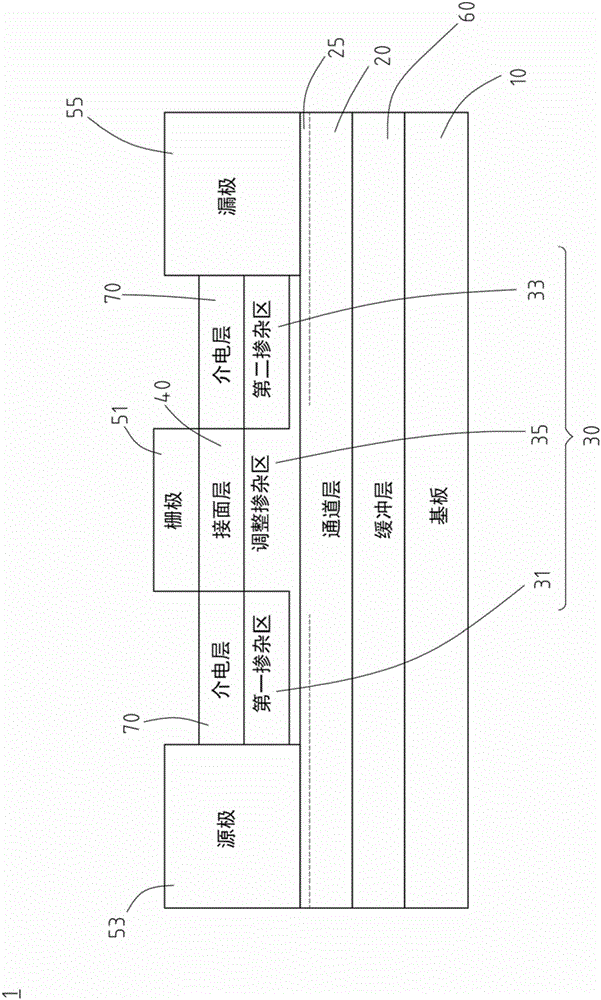
[0048] refer to figure 1 , a schematic cross-sectional view of the enhanced high electron mobility transistor structure of the present invention. like figure 1 As shown, the enhanced high electron mobility transistor structure 1 includes a substrate 10 , a channel layer 20 , a barrier layer 30 , a junction layer 40 , a gate 51 , a source 53 , and a drain 55 . The substrate 10 is a silicon substrate, a sapphire substrate or a silicon carbide (SiC) substrate. The channel layer 20 is located on the substrate 10 and is made of a first III-V semiconductor, such as intrinsic gallium nitride (i-GaN). The barrier layer 30 is disposed on the channel layer 20 and is made of a second III-V semiconductor, and the second III-V semiconductor is different from the first III-V semiconductor. Due to the difference in material energy levels a...


PUM


Abstract

An enhancement-mode high-electron-mobility transistor structure comprises a channel layer, a barrier layer, an interface layer, a gate electrode, a source electrode and a drain electrode. The channel layer is a first III-V semiconductor and is arranged on a substrate. The barrier layer is a second III-V semiconductor and is arranged on the channel layer. The barrier layer comprises a first doped region, an adjusting doped region and a second doped region. The first doped region and the second doped region are n-type second III-V semiconductor, and the adjusting doped region comprises a p-type second III-V semiconductor. The first doped region and the second doped region are arranged at two sides of the adjusting doped region. The interface layer is arranged above the adjusting doped region and is a p-type third III-V semiconductor, and furthermore the doping amount is higher than that of the adjusting doped region. Furthermore the doping concentration of an area which is adjacent to the interface area in the adjusting doped region is higher than that of the area that is adjacent to the channel layer.

Description

technical field [0001] The invention relates to a semiconductor structure, in particular to an enhanced high electron mobility transistor structure. Background technique [0002] A high-electron-mobility transistor (High-Electron-Mobility Transistor, HEMT) is an improvement on a metal-oxide-semiconductor field-effect transistor (MOSFET). The main feature is the use of two semiconductor materials with different energy gaps. It is common to join two III-V semiconductors in an epitaxial manner, such as gallium arsenide (GaAs), gallium nitride (GaN), arsenide Aluminum Gallium (Al x Ga 1-x As), aluminum gallium nitride (Al x Ga 1-x N), indium gallium nitride, etc. (In x Ga 1-x N), forming a carrier channel between the interfaces. [0003] The movement of carriers is limited to two dimensions by the quantum well, so it is also called two-dimensional electron gas (Two-Dimension Electron Gas, 2DEG). Due to the reduction of one-dimensional scattering, the mobility of electron...

Claims


Application Information

Patent Timeline
Patent Type & Authority Applications(China)
IPC IPC(8): H01L29/778H01L29/06
CPCH01L29/0607H01L29/0611H01L29/0684H01L29/7783H01L29/7789
Inventor 黄彦纶孙健仁李依晴徐文庆
Owner GLOBALWAFERS CO LTD
Why Eureka
Try Eureka