A gate-controlled semiconductor device with a new gate structure
A gate structure and semiconductor technology, applied in semiconductor devices, electrical components, circuits, etc., can solve the problems of affecting the frequency characteristics of devices, reducing transconductance, increasing the distance from gate to channel with insulating gate dielectric, etc., to increase gate control ability, The effect of increasing the breakdown voltage and operating frequency and reducing the gate leakage current
- Summary
- Abstract
- Description
- Claims
- Application Information
AI Technical Summary
Problems solved by technology
Method used
Image

Examples
Embodiment 1
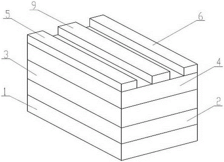
[0024] Such as Figure 3 to Figure 5 As shown, a III-nitride HEMT with a new gate structure includes substrate 1, buffer layer 2, channel layer 3 and barrier layer 4 from bottom to top, buffer layer 2, channel layer 3 and barrier layer Layer 4 is equivalent to the middle layer, and the source electrode 5 and the drain electrode 6 are made on the barrier layer 4, and a gate structure is arranged between the source electrode 5 and the drain electrode 6, and the gate structure is composed of dielectric gates and dielectric gates alternately connected along the gate width direction. The Schottky grid is composed of a dielectric grid metal 8 and a gate dielectric 7 arranged up and down. In this embodiment, there are 4 dielectric gates and 3 Schottky gates, and the two ends of the gate structure are dielectric gates.
[0025] The substrate 1 is Si or sapphire or SiC or GaN or diamond.
[0026] The buffer layer 2 is AlN or GaN or AlN and Al x Ga 1-x N (0x Al 1-x N (0
[0...
Embodiment 2
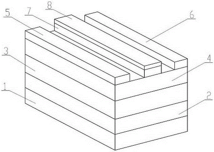
[0035] Depend on Figure 6 It can be seen that, different from Embodiment 1, this embodiment is a delta-doped gate-controlled semiconductor device with a novel gate structure, the middle layer is an N-type or P-type delta-doped semiconductor 10, and the two ends of the gate structure One end is a dielectric grid, and the other end is a Schottky grid.
[0036] In this embodiment, the widths of the dielectric gates are equal, and the widths of the Schottky gates are equal, but the widths of the two are not equal.
[0037] In this embodiment, the dielectric grid and the Schottky grid are planar grids.
Embodiment 3
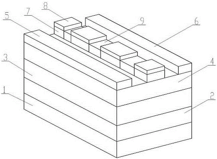
[0039] Depend on Figure 7 It can be seen that, different from Embodiment 1, the dielectric grid in this embodiment is a grooved grid, and the Schottky grid is a planar grid. Of course, the Schottky gate can also be a grooved gate, that is, both the dielectric gate and the Schottky gate are grooved gates. The groove depths of the dielectric grids or Schottky grids may be equal or unequal.
PUM
 Abstract
Description
Claims
Application Information
 - R&D
- Intellectual Property
- Life Sciences
- Materials
- Tech Scout
- Unparalleled Data Quality
- Higher Quality Content
- 60% Fewer Hallucinations
Browse by: Latest US Patents, China's latest patents, Technical Efficacy Thesaurus, Application Domain, Technology Topic, Popular Technical Reports.
© 2025 PatSnap. All rights reserved.Legal|Privacy policy|Modern Slavery Act Transparency Statement|Sitemap|About US| Contact US: help@patsnap.com