Method for preparing crystalline silicon dual-emitter back knot and back contact solar cell

A technology of solar cells and double emitters, applied in circuits, electrical components, semiconductor devices, etc., can solve problems such as cost increase, inconsistent boron and phosphorus injection activation conditions, etc., to save time and heat loss, excellent quality and performance, avoid The effect of mutual influence

Active Publication Date: 2013-11-20
INST OF MICROELECTRONICS CHINESE ACAD OF SCI
View PDF2 Cites 5 Cited by
  • Summary
  • Abstract
  • Description
  • Claims
  • Application Information

AI Technical Summary

Problems solved by technology

However, multi-step ion implantation will lead to a substantial increase in cos...

Method used


Image

  • Method for preparing crystalline silicon dual-emitter back knot and back contact solar cell
  • Method for preparing crystalline silicon dual-emitter back knot and back contact solar cell
  • Method for preparing crystalline silicon dual-emitter back knot and back contact solar cell

Examples


Embodiment Construction

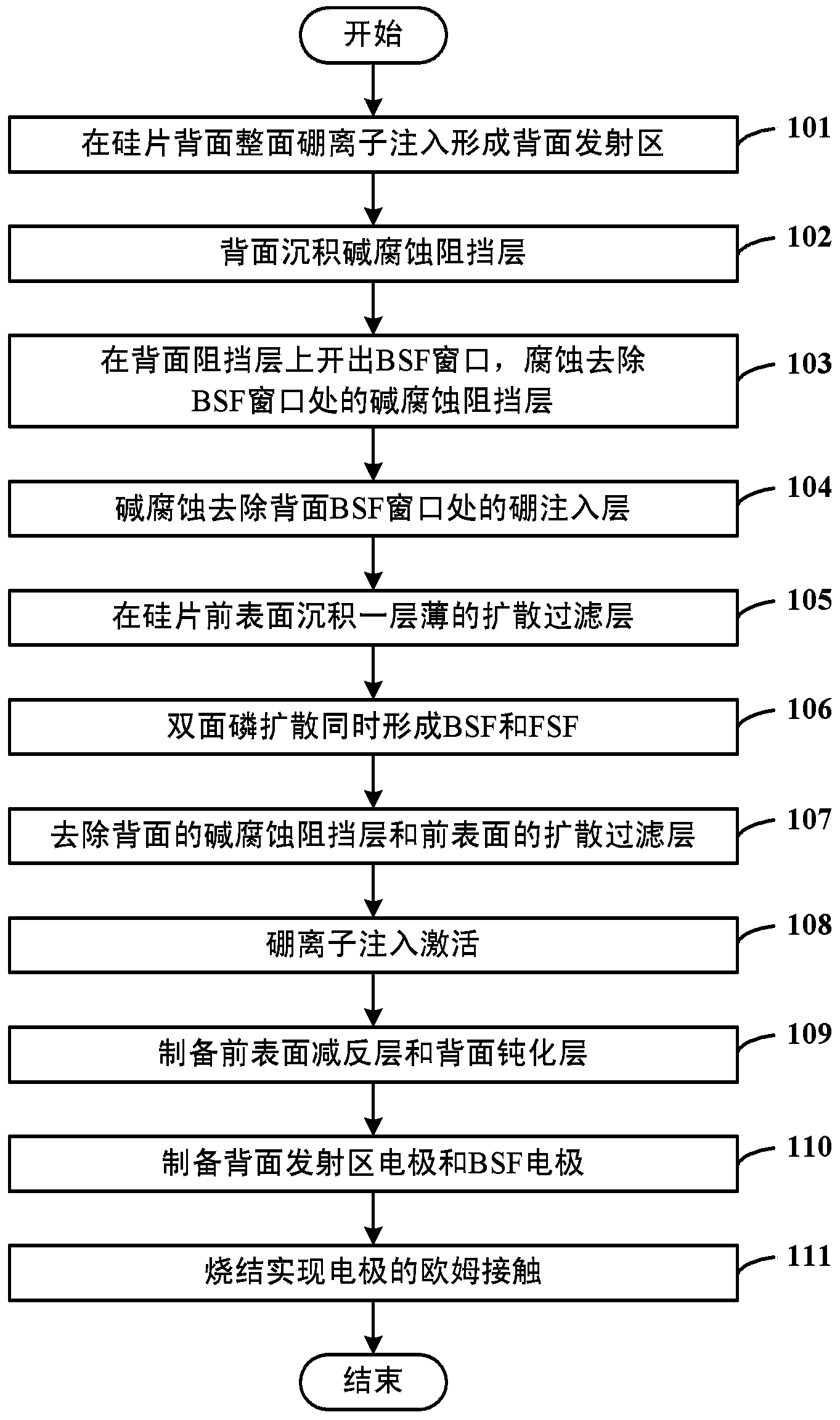
[0051] In order to further explain the technical means and effects that the present invention takes to achieve the intended purpose of the invention, the method for preparing double-emitter back-junction back-contact solar cells according to the boron ion implantation proposed by the present invention will be described below in conjunction with the accompanying drawings and preferred embodiments. The specific embodiment, structure, feature and effect thereof are described in detail as follows.

[0052] Such as figure 1 as shown, figure 1 It is a flow chart of a method for preparing a crystalline silicon double-emitter back-junction back-contact solar cell provided by the invention, and the method may further comprise the steps:

[0053] Step 101: implanting boron ions on the back of the silicon wafer to form a back emission region;

[0054] Step 102: Depositing an alkali corrosion barrier layer on the back;

[0055] Step 103: Open a BSF window on the back barrier layer, and...


PUM

PropertyMeasurementUnit
Resistivityaaaaaaaaaa
Thicknessaaaaaaaaaa

Abstract

The invention discloses a method for preparing a crystalline silicon dual-emitter back knot and back contact solar cell, which comprises the steps that boron ion implantation is conducted on the whole back surface of a silicon wafer to form a back surface emitting area; an alkali corrosion barrier layer is deposited on the back surface; a BSF (Back Surface Field) window is opened on a back surface barrier layer; the alkali corrosion barrier layer at the BSF window is removed by corrosion; a boron implantation layer at the BSF window is removed by alkali corrosion; a thin diffusion filter layer is deposited on the front surface of the silicon wafer; double-surfaced phosphorus is diffused; a BSF and an FSF (Front Surface Field) are formed simultaneously; the back surface alkali corrosion barrier layer and the front surface diffusion filter layer are removed; the boron ion implantation is activated; a front surface decreasing layer and a back surface passivation layer are prepared; a back surface emitting area electrode and a BSF electrode are prepared; and ohmic contact of the electrodes is achieved by sintering. According to the method, a technique is simplified; the performance is improved; and the method has very great benefits to an industrial prospect of the dual-emitter back knot and back contact cell.

Description

technical field [0001] The invention relates to the technical field of solar cell manufacturing, in particular to a method for preparing a crystalline silicon double-emitter back-junction back-contact high-efficiency solar cell based on boron ion implantation. Background technique [0002] Low cost and high efficiency have always been the direction pursued by solar cells. However, in conventional solar cell structures, the front-surface silver electrodes lead to severe light-shielding loss. Severe series resistance losses occur on the welding strips between the cells when forming the module, resulting in a module whose efficiency is much lower than that of a single cell. For this reason, the double-emitter back-junction back-contact battery transfers both the positive and negative electrodes to the back of the battery, and the shading loss of the electrodes on the front surface is zero. In addition, the interconnection of the battery sheets in the double-emitter back-junct...

Claims


Application Information

Patent Timeline
IPC IPC(8): H01L31/18
CPCY02P70/50
Inventor 贾锐邢钊陈晨张巍张代生金智刘新宇
Owner INST OF MICROELECTRONICS CHINESE ACAD OF SCI
Why Eureka
Try Eureka