AMOLED (active matrix organic light emitting diode) and manufacturing method thereof

A technology of light-emitting diodes and manufacturing methods, which is applied in semiconductor/solid-state device manufacturing, electrical components, electric solid-state devices, etc., can solve problems such as low luminous efficiency, achieve high luminous efficiency, high stability, and improve the effect of electron injection efficiency

Active Publication Date: 2013-11-20
TRULY SEMICON
View PDF2 Cites 14 Cited by
  • Summary
  • Abstract
  • Description
  • Claims
  • Application Information

AI Technical Summary

Problems solved by technology

[0006] However, in the process of practical application, it is found that the luminous efficiency of AMOLED made of OLED with inverted structure is low.

Method used


Image

  • AMOLED (active matrix organic light emitting diode) and manufacturing method thereof
  • AMOLED (active matrix organic light emitting diode) and manufacturing method thereof
  • AMOLED (active matrix organic light emitting diode) and manufacturing method thereof

Examples


Embodiment 1

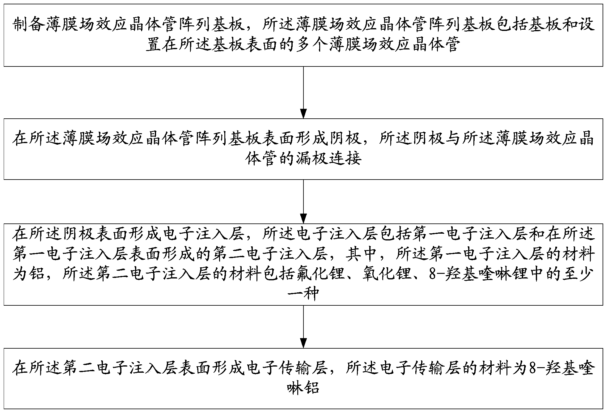
[0044] This embodiment provides a method for manufacturing an active matrix organic light emitting diode panel, such as figure 2 As shown, the method includes:

[0045] preparing a thin film field effect transistor array substrate, the thin film field effect transistor array substrate comprising a substrate and a plurality of thin film field effect transistors arranged on the surface of the substrate;

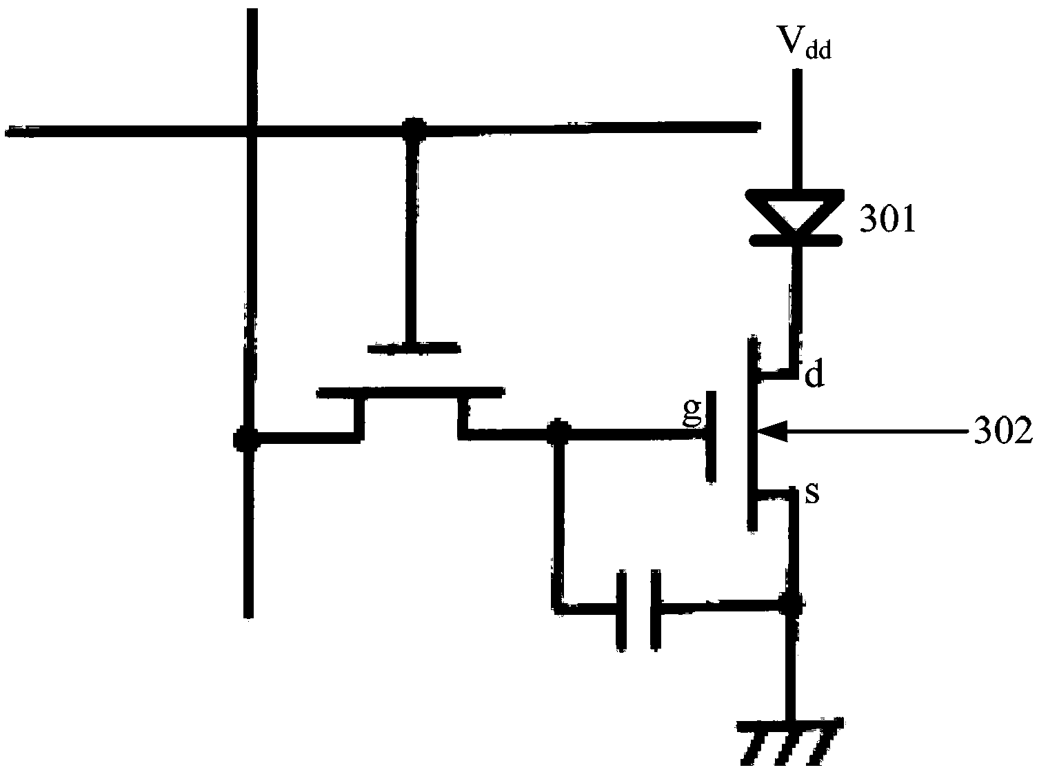
[0046] One of the formation methods of a single TFT is: first form a gate on the substrate, then form a gate insulating layer or an etching barrier layer that completely covers the gate on the gate, and then form a gate insulating layer or an etching barrier layer on the surface of the gate insulating layer or etching barrier layer. An active layer is formed on the active layer, and then a source electrode and a drain electrode are formed on the active layer, and finally a passivation layer is covered on the source electrode and the drain electrode, and a drain contact hole ex...

Embodiment 2

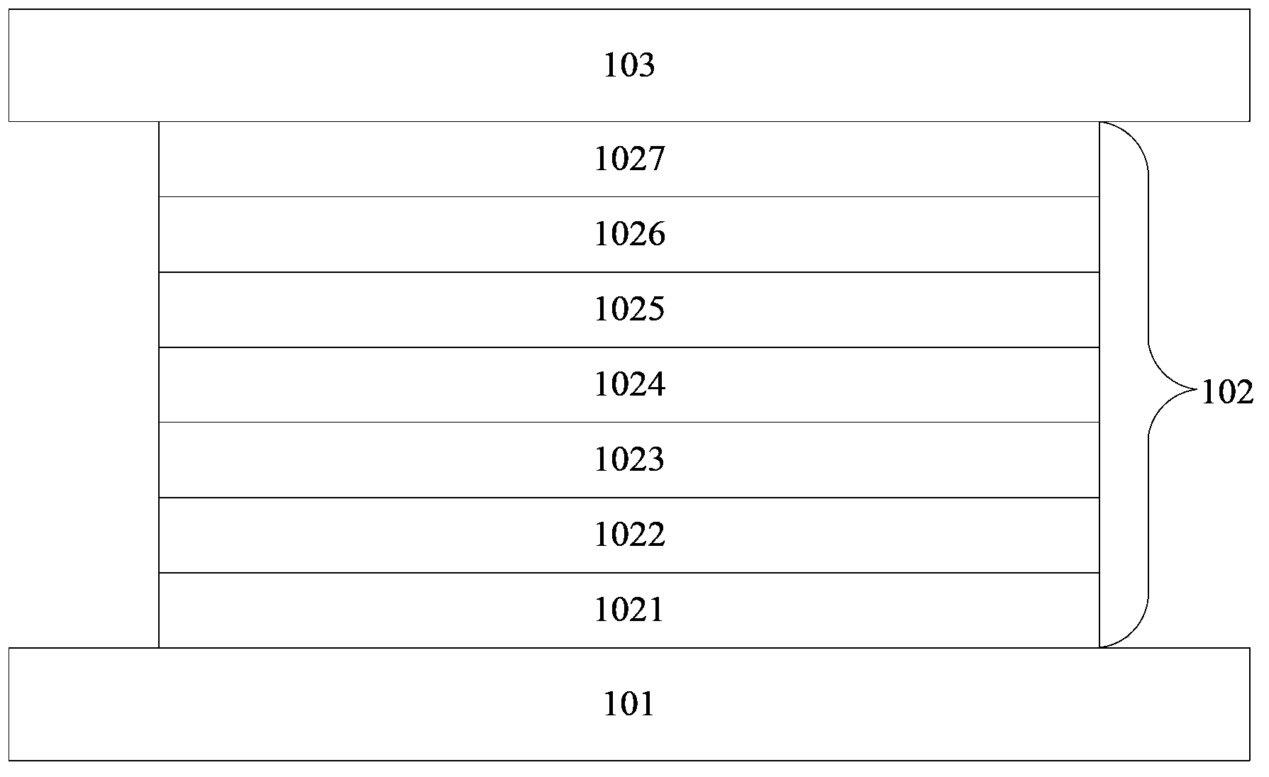
[0085] Based on Embodiment 1, this embodiment provides an active matrix organic light-emitting diode panel, which is produced by the manufacturing method provided in Embodiment 1. The device includes:

[0086] A thin film field effect transistor array substrate, the thin film field effect transistor array substrate comprising a substrate and a plurality of thin film field effect transistors arranged on the surface of the substrate;

[0087] a cathode located on the surface of the thin film field effect transistor array substrate, the cathode is connected to the drain of the thin film field effect transistor;

[0088] An electron injection layer located on the surface of the cathode, the electron injection layer comprising a first electron injection layer located on the surface of the cathode and adjacent to the cathode and a second electron injection layer located on the surface of the first electron injection layer , the first electron injection layer is an aluminum layer, an...


PUM


Abstract

The invention provides an AMOLED (active matrix organic light emitting diode) and a manufacturing method of the AMOLED. The manufacturing method comprises the following steps of manufacturing a TFT (thin film transistor) array substrate; forming a cathode on the surface of the FTF array substrate; forming an electron injection layer on the surface of the cathode, wherein the electron injection layer comprises a first electron injection layer and a second electron injection layer formed on the surface of the first electron injection layer, the first electron injection layer is made of aluminum, and the second electron injection layer is made from at least one of LiF, Li2O and Liq; and forming an electronic transfer layer on the surface of the second electron injection layer, wherein the electronic transfer layer is made from 8-hydroxyquinoline. According to the AMOLED and the manufacturing method of the AMOLED, which are disclosed by the invention, the material of the electron injection layer is resolved under the coexistence of Al and Alq3 to generate Li<+>Alq3<-> to modify an interface between the Al and the Alq3 to cause band bending of the Alq3, so that electrons in the cathode can more easily be injected into the electronic transfer layer; and therefore, the electron injection efficiency is improved, and the light emitting efficiency of the AMOLED is improved.

Description

technical field [0001] The invention relates to the technical field of light-emitting diodes, and more specifically, relates to an active matrix organic light-emitting diode panel and a manufacturing method thereof. Background technique [0002] Active Matrix Organic Light Emitting Diode (AMOLED) is a display technology that has received extensive attention at present. It has self-illumination, high brightness, high contrast, wide viewing angle, fast response, low power consumption, Light and thin and many other advantages, it is called the next generation of display technology. [0003] AMOLED has a pixel array composed of a plurality of pixel units, each of which includes an organic light emitting diode (Organic Light Emitting Diode, OLED for short) and a thin film field effect transistor (Thin Film Transistor, TFT for short). Among them, OLED uses organic semiconductor materials and light-emitting materials to emit light through carrier injection and recombination under ...

Claims


Application Information

Patent Timeline
Patent Type & Authority Applications(China)
IPC IPC(8): H01L51/56H01L27/32H01L51/50H01L51/54
Inventor 何剑何基强苏君海柯贤军
Owner TRULY SEMICON
Why Eureka
Try Eureka