

Defect detection system for extreme ultraviolet lithography mask
A technology for extreme ultraviolet lithography and defect detection, applied in the field of extreme ultraviolet lithography mask defect detection system, to achieve the effects of small size, easy processing, and reduced processing costs
- Summary
- Abstract
- Description
- Claims
- Application Information
AI Technical Summary
Problems solved by technology
Method used
Image

Examples
Embodiment Construction
[0021] In order to make the object, technical solution and advantages of the present invention clearer, the present invention will be described in further detail below in conjunction with specific embodiments and with reference to the accompanying drawings.
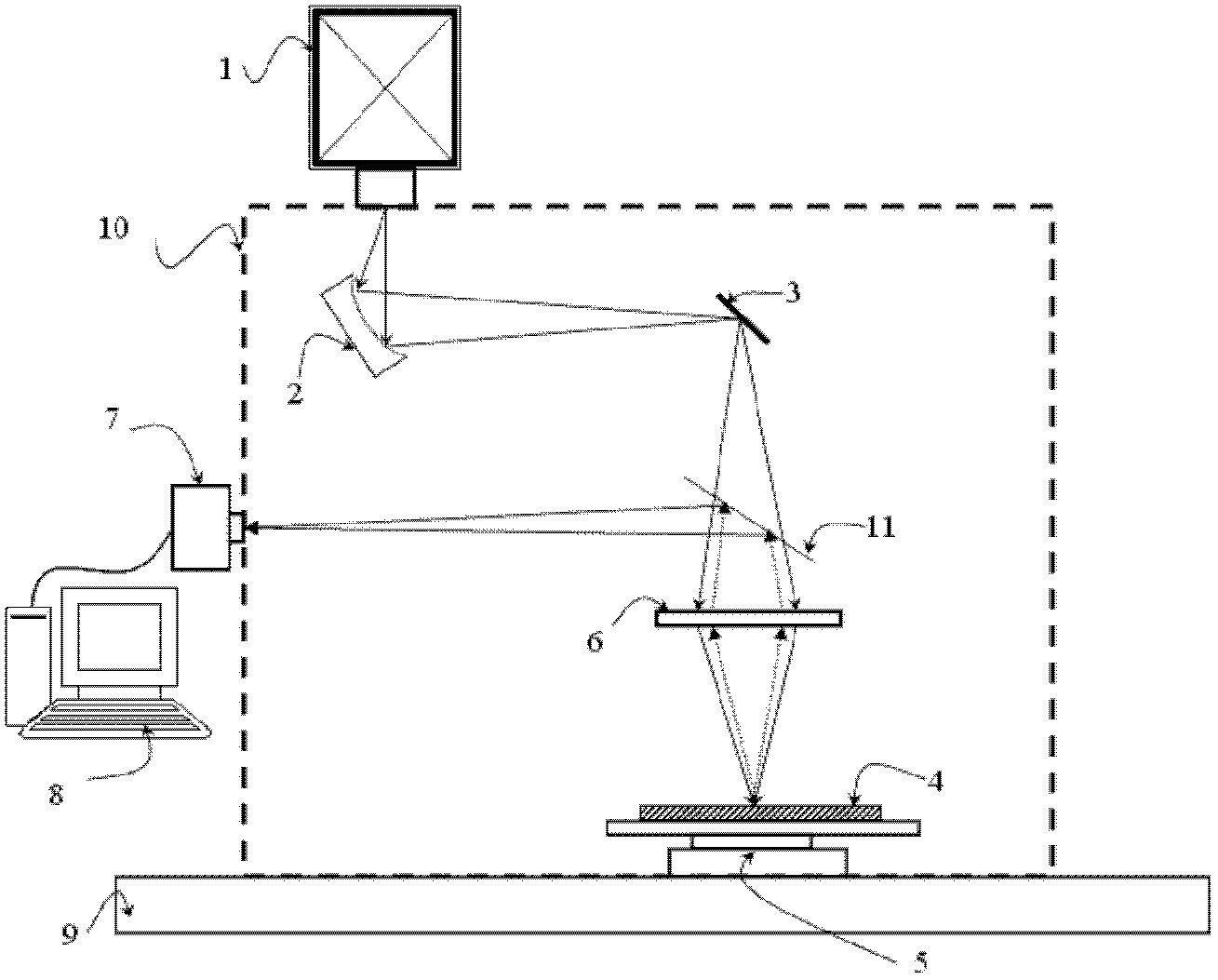
[0022] The EUV lithography mask defect detection system provided by the present invention uses a photon sieve instead of a traditional Schwarzchild objective to realize imaging of the mask in the EUV band, thereby detecting defects on the mask.
[0023] like figure 1 as shown, figure 1 It is a schematic structural diagram of an extreme ultraviolet lithography mask defect detection system according to an embodiment of the present invention. The extreme ultraviolet lithography mask defect detection system is oriented to the detection of mask defects in extreme ultraviolet lithography at the 22nm node, and specifically includes extreme ultraviolet lithography. Light source 1, extreme ultraviolet light transmission system (i...
PUM
| Property | Measurement | Unit |
|---|---|---|
| power | aaaaa | aaaaa |
| thickness | aaaaa | aaaaa |
| diameter | aaaaa | aaaaa |
Abstract
Description
Claims
Application Information