Flash memory cell and method of forming same

A flash memory cell and material layer technology, which is applied in the manufacture of electrical components, electric solid-state devices, and semiconductor/solid-state devices, etc., can solve the problems of low erasing and writing efficiency and low coupling efficiency of flash memory, and improve the erasing and writing performance and coupling efficiency. , the effect of increasing the capacitance

Active Publication Date: 2016-09-28
SHANGHAI HUAHONG GRACE SEMICON MFG CORP
View PDF4 Cites 0 Cited by
  • Summary
  • Abstract
  • Description
  • Claims
  • Application Information

AI Technical Summary

Problems solved by technology

[0006] The coupling efficiency of the control gate to the floating gate of the existing flash memory is low, and the erasing and writing efficiency of the flash memory is low, which needs to be further improved

Method used


Image

  • Flash memory cell and method of forming same
  • Flash memory cell and method of forming same
  • Flash memory cell and method of forming same

Examples


Embodiment Construction

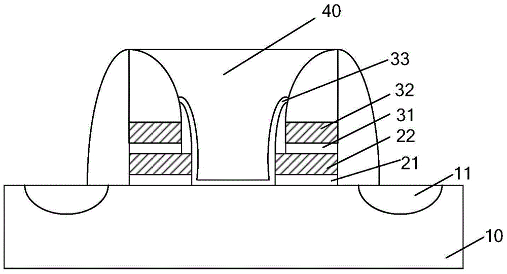
[0023] As mentioned in the background, the coupling efficiency of the control gate to the floating gate in the flash memory formed in the prior art is not high. Studies have found that this low coupling efficiency will cause the floating gate to be coupled with a low voltage from the control gate, resulting in the need to increase the voltage to a very high level when programming or erasing the flash memory, reducing the erasing efficiency of the flash memory, and reducing the performance of the flash memory. The consumption becomes larger, and the higher voltage will also increase the requirements for material reliability.

[0024] The control gate-to-floating gate coupling efficiency of a flash memory is the ratio of the capacitance between the control gate and the floating gate to the total capacitance around the floating gate. The control gate of the prior art flash memory is located above the top surface of the floating gate. The capacitance between the gates depends on t...


PUM


Abstract

Disclosed are a flash memory unit and a formation method thereof. The formation method of the flash memory unit includes the steps: providing a semiconductor substrate and forming a first dielectric layer and a floating gate material layer of the surface of the first dielectric layer on the surface of the semiconductor substrate; forming a second dielectric layer and a control gate material layer of the surface of the second dielectric layer covering the first dielectric layer and the floating gate material layer; forming a hard mask layer with an opening on the surface of the control gate material layer; forming a first side wall in the opening; etching the control gate material layer by taking the first side wall and the hard mask layer as masks to form a first groove; forming a second side wall positioned on the side wall of the control gate material layer in the first groove; etching the second dielectric layer, the floating gate material layer and the first dielectric layer along the first groove to form a second groove and a floating gate; forming a tunneling oxide layer on the surface of the inner wall of the second groove; forming word lines filled in the first groove and the second groove on the surface of the tunneling oxide layer. By the method, the coupling efficiency of a control gate for the floating gate in a flash memory can be improved, so that the erasing performance of the flash memory is improved.

Description

technical field [0001] The invention relates to the technical field of semiconductors, in particular to a flash memory unit and a forming method thereof. Background technique [0002] In the current semiconductor industry, integrated circuit products can be mainly divided into three types: logic, memory and analog circuits, among which storage devices account for a considerable proportion of integrated circuit products, such as RAM (random access memory), DRAM (dynamic Random access memory), ROM (read-only memory), EPROM (erasable programmable read-only memory), FLASH (flash memory) and FRAM (ferroelectric memory), etc. [0003] In memory, the development of flash memory is particularly rapid. Its main feature is that it can keep the stored information for a long time without power on. It has many advantages such as high integration, fast access speed and easy erasure, so it has been widely used in many fields such as microcomputer and automatic control. a wide range of ap...

Claims


Application Information

Patent Timeline
Patent Type & Authority Patents(China)
IPC IPC(8): H01L21/8247H01L27/115
Inventor 于涛
Owner SHANGHAI HUAHONG GRACE SEMICON MFG CORP
Why Eureka
Try Eureka