Low-refractivity waveguide modulator for graphene and preparing method

A waveguide modulator, low-refractive index technology, applied in instruments, nonlinear optics, optics, etc., can solve the problems of weak electro-optical characteristic size, difficult silicon-based integration, narrow modulation spectral range, etc., and achieves improved spectral design freedom, Improved modulation depth, effect of large test alignment tolerance

Inactive Publication Date: 2013-12-11
INST OF SEMICONDUCTORS - CHINESE ACAD OF SCI
View PDF6 Cites 28 Cited by
  • Summary
  • Abstract
  • Description
  • Claims
  • Application Information

AI Technical Summary

Problems solved by technology

At present, traditional silicon-based electroabsorption modulators are large in size due to weak electro-optical characteristics; germanium and other compound semiconductor modulators are difficult to integrate on silicon; their modulation spectral range is usually relatively narrow

Method used


Image

  • Low-refractivity waveguide modulator for graphene and preparing method
  • Low-refractivity waveguide modulator for graphene and preparing method
  • Low-refractivity waveguide modulator for graphene and preparing method

Examples


Embodiment Construction

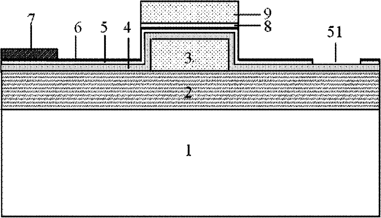
[0035] see figure 1 As shown, the present invention provides a graphene electric absorption low refractive index difference waveguide modulator, comprising:

[0036] A substrate 1, the substrate 1 is made of single crystal silicon, which is easy to integrate with other silicon-based devices;

[0037] The lower cladding layer 2 is made on the substrate 1, the material of the lower cladding layer 2 is silicon oxide with a low refractive index, its refractive index is 1.445, and its thickness is 15-20 microns. The lower cladding layer 2 is used to prevent the The light field of the core layer leaks to the substrate;

[0038] A waveguide core layer 3, which is fabricated in the middle of the lower cladding layer 2, forming a ridge structure with a width of 6 microns;

[0039] An ITO transparent electrode 4, which is made on the waveguide core layer 3 and both sides, and covers the upper surface of the exposed lower cladding layer 2, the material of the ITO transparent electrode ...


PUM

PropertyMeasurementUnit
thicknessaaaaaaaaaa
widthaaaaaaaaaa
thicknessaaaaaaaaaa

Abstract

The invention provides a low-refractivity waveguide modulator for graphene. The low-refractivity waveguide modulator comprises a substrate, lower cladding, a waveguide core layer, an ITO transparent electrode, a lower insulating medium layer, a single-layer graphene film, a metal electrode, an upper insulating medium layer and a high refractive index silicon oxide layer, wherein the lower cladding is arranged on the substrate, the waveguide core layer is arranged in the middle of the lower cladding for forming a ridge-shaped structure, the ITO transparent electrode is arranged on the waveguide core layer and the two sides and covers the exposed upper surface of the lower cladding, the lower insulating medium layer is arranged on the surface of the ITO transparent electrode, the portion, on one side of the ridge-shaped structure, of the insulating medium layer is of a disconnection shape and forms a window, the single-layer graphene film is arranged on the lower insulating medium layer, the metal electrode is arranged on one side of the ridge-shaped structure and the single-layer graphene film of the other side far away from the window, the preset distance larger than 800nm is kept between the metal electrode and the ridge-shaped structure, the upper insulating layer is arranged on the single-layer graphene film on the ridge-shaped structure, and the high refractive index silicon oxide layer is arranged on the upper insulating medium layer. The low-refractivity waveguide modulator has the advantages of being small in size, wide in modulation bandwidth, low in insertion loss and simple in preparing process.

Description

technical field [0001] The invention belongs to the technical field of semiconductors, in particular to a waveguide modulator with low refractive index difference of graphene and a preparation method thereof. Background technique [0002] Optical fiber communication technology is the main form of modern communication, which has the characteristics of high speed, low loss, wide frequency and high reliability. Optical modulators play a vital role in the modulation of optical signals in optical fiber communications. The role of optical modulation technology is to load bit signals onto optical waves, and generate modulated optical pulses through continuous switching. It is through the voltage A device that modulates the absorptivity, refractive index, phase or amplitude of the output light by changing the electric field. According to various forms of electro-optic, acousto-optic, magneto-optical effects, quantum well Stark effect and carrier dispersion effect, etc., it regulate...

Claims


Application Information

Patent Timeline
Patent Type & Authority Applications(China)
IPC IPC(8): G02F1/025
Inventor 尹伟红韩勤杨晓红李彬崔荣吕倩倩
Owner INST OF SEMICONDUCTORS - CHINESE ACAD OF SCI
Why Eureka
Try Eureka