Rolled copper or copper-alloy foil provided with roughened surface
A technology for roughening the surface and copper alloy foil. It is applied in the direction of thin material processing, secondary processing of printed circuits, metal pattern materials, etc. It can solve the problems of copper foil etching damage and undercut, and achieve high peel strength. , good etching and gloss, with acid resistance and tin plating solution resistance effect
- Summary
- Abstract
- Description
- Claims
- Application Information
AI Technical Summary
Problems solved by technology
Method used
Image
Examples
Embodiment 1
[0077] As the copper foil, a rolled copper alloy foil composed of Cr: 0.2% by weight, Zr: 0.1% by weight, Zn: 0.2% by weight, and the balance of Cu and unavoidable impurities was used.
[0078] The rolled copper foil was subjected to degreasing and water washing treatment, followed by pickling and water washing treatment, and then, copper sulfate (Cu: 20g / L in conversion), sulfuric acid: 100g / L, temperature: 50°C, Dk: 5.0A / dm 2 (C: 10.3As / dm 2 ) under the conditions of forming a 0.04μm thick copper base plating. The thickness of the base plating layer is a trial value obtained from the Coulomb quantity and the specific gravity of copper.
[0079] Next, on the base coating, further at Dk: 50A / dm 2 (C: 70As / dm 2 ) conditions, the roughening treatment was performed by copper plating treatment including copper particles of 0.4 μm.
[0080] Various evaluation tests were performed on the rolled copper alloy foil after the roughening plating under the conditions shown below. I...
Embodiment 2
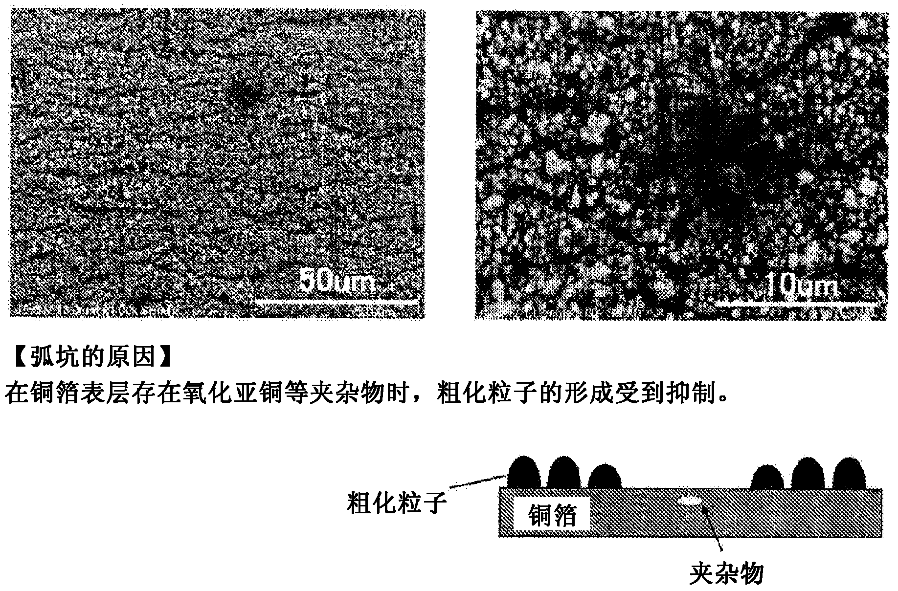
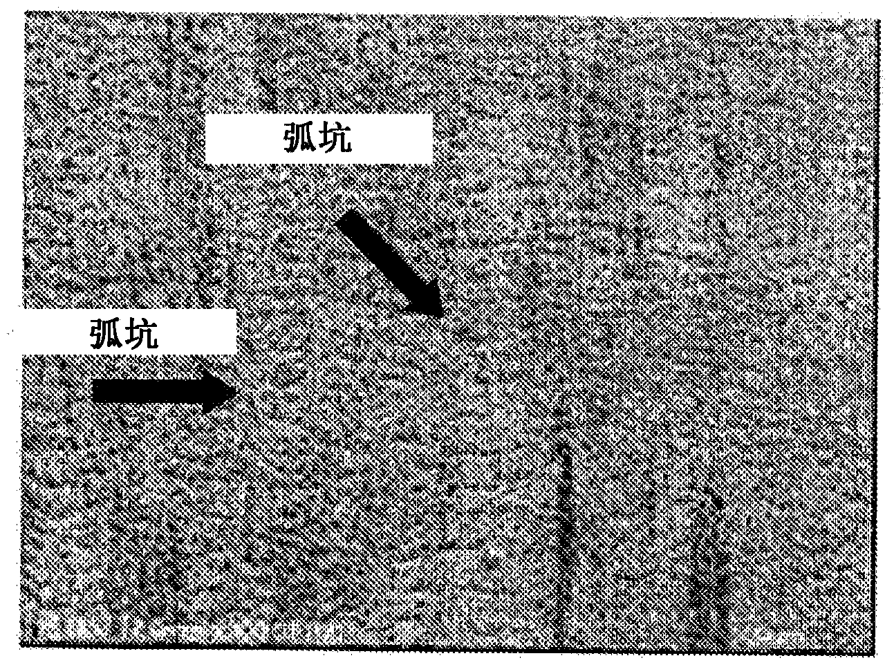
[0087] The formation condition of the copper base plating layer is Dk: 10.0A / dm 2 (C: 20.7As / dm 2 ) under the condition of forming a 0.08μm thick base plating layer of copper. Other conditions are identical with embodiment 1. The number of craters on the copper roughened surface was counted with an optical microscope, and the number was investigated. The results are similarly shown in Table 1 above. As shown in Table 1, in Example 2, the generation of arc craters is less, 2.1 craters / 25mm 2 .
Embodiment 3
[0089] The formation condition of the copper base plating layer is Dk: 15.0A / dm 2 (C: 41.0As / dm 2 ) under the condition of forming a 0.15 μm thick copper base plating. Other conditions are identical with embodiment 1. The number of craters on the copper roughened surface was counted with an optical microscope, and the number was investigated. The results are similarly shown in Table 1 above. As shown in Table 1, in Example 3, the generation of arc craters is less, 0.5 craters / 25mm 2 .
PUM
| Property | Measurement | Unit |
|---|---|---|
| area | aaaaa | aaaaa |
| diameter | aaaaa | aaaaa |
| current density | aaaaa | aaaaa |
Abstract
Description
Claims
Application Information


