Pt/silicon nanometer array structure composite material and preparation method thereof

A technology of silicon nanoarray and composite material, applied in the field of Pt/silicon nanoarray structure composite material and its preparation, can solve the problems of secondary chemical damage, increase of surface defects, unfavorable photoelectric energy conversion, etc., and achieve effective absorption and conversion, Effect of reducing recombination centers, good visible light absorption

Inactive Publication Date: 2013-12-25
CHONGQING UNIV
View PDF2 Cites 4 Cited by
  • Summary
  • Abstract
  • Description
  • Claims
  • Application Information

AI Technical Summary

Problems solved by technology

However, in the introduction of the catalyst, the traditional method is to use silicon to directly reduce the metal (Galvanic displacement) in a fluorine-containing solution, but this produces secondary chemical damage, which increases the surface defects of the silicon matrix material, and these defects will become The recombination center of photogenerated electrons and holes is not conducive to photoelectric energy conversion

Method used


Image

  • Pt/silicon nanometer array structure composite material and preparation method thereof
  • Pt/silicon nanometer array structure composite material and preparation method thereof
  • Pt/silicon nanometer array structure composite material and preparation method thereof

Examples


Embodiment 1

[0042] 1. Preparation of silicon nanowire arrays:

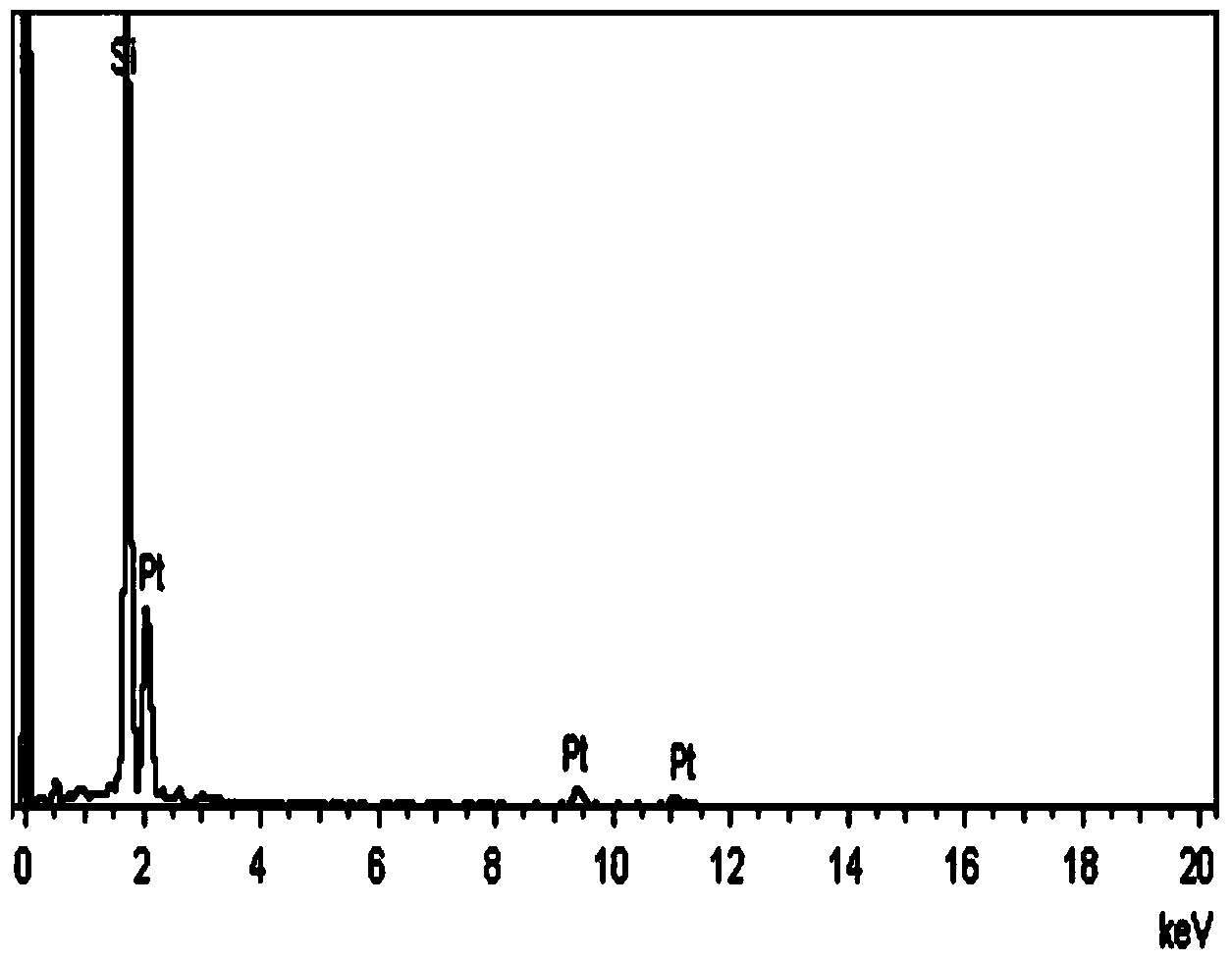
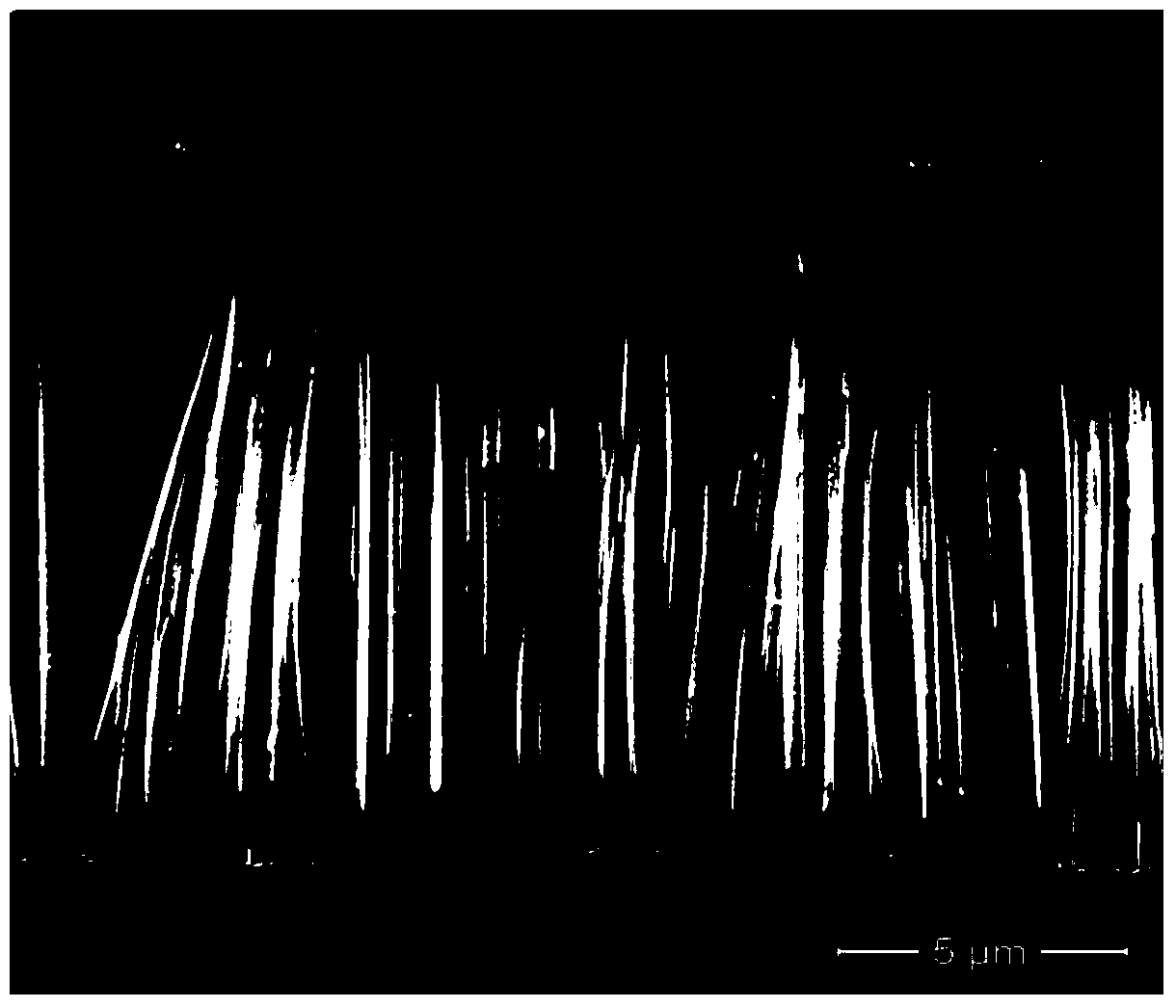
[0043] Cut the p-type Si wafer into 1 × 2 cm 2 The squares were ultrasonically washed with deionized water, absolute ethanol and acetone, and then immersed in H 2 SO 4 and H 2 o 2 Take out after 10 minutes in the mixed solution (mixed solution by H 2 SO 4 (98%) and H 2 o 2 (35%) configured according to the volume ratio of 3:1). The silicon wafer was placed in a 5% HF aqueous solution, allowed to stand for 1 minute, and then taken out. The silicon wafer was rapidly transferred to a solution containing 4.8M HF and 5mM AgNO 3 In the mixed solution, stir slowly, and take it out after 60 seconds of reaction. Then transfer the silicon wafer to 4.8M HF and 0.25mM H 2 o 2 In the solution, react for 45 minutes under the condition of avoiding light, and obtain the silicon nanowire array. Next, the silicon nanowire arrays were transferred into nitric acid solution (V HNO3(63%) :V 水 =1:1) for 3 hours, remove Ag ions, and t...

Embodiment 2

[0048] 1. Preparation of porous silicon nanoarray structure:

[0049] Cut the p-type Si wafer into 1 × 2 cm 2 The squares were ultrasonically washed with deionized water, absolute ethanol and acetone, and then immersed in H 2 SO 4 and H 2 o 2 Take out after 10 minutes in the mixed solution (mixed solution by H 2 SO 4 (98%) and H 2 o 2 (35%) configured according to the volume ratio of 3:1). The silicon wafer was placed in a 5% HF aqueous solution, allowed to stand for 1 minute, and then taken out. The silicon wafer was rapidly transferred to a solution containing 4.8M HF and 5mM AgNO 3 In the mixed solution, stir slowly, and take it out after 60 seconds of reaction. Then transfer the silicon wafer to 4.8M HF and 0.25mM H 2 o 2 In the solution, react for 10 minutes under the condition of avoiding light, and obtain the porous silicon nano-array. Next, the porous silicon nanoarrays were transferred into nitric acid solution (V HNO3(63%) :V 水 =1:1) for 3 hours, remov...

Embodiment 3

[0053] 1. Preparation of silicon nanowire arrays:

[0054] Cut the n-type Si wafer into 1 × 2 cm 2 The squares were ultrasonically washed with deionized water, absolute ethanol and acetone, and then immersed in H 2 SO 4 and H 2 o 2 Take out after 10 minutes in the mixed solution (mixed solution by H 2 SO 4 (98%) and H 2 o 2 (35%) configured according to the volume ratio of 3:1). The silicon wafer was placed in a 5% HF aqueous solution, allowed to stand for 1 minute, and then taken out. The silicon wafer was rapidly transferred to a solution containing 4.8M HF and 5mM AgNO 3 In the mixed solution, stir slowly, and take it out after 60 seconds of reaction. Then transfer the silicon wafer to 4.8M HF and 0.25mM H 2 o 2 In the solution, react for 45 minutes under the condition of avoiding light, and obtain the silicon nanowire array. Next, the silicon nanowire arrays were transferred into nitric acid solution (V HNO3(63%) :V 水 =1:1) for 3 hours, remove Ag ions, and t...


PUM

PropertyMeasurementUnit
diameteraaaaaaaaaa
diameteraaaaaaaaaa
concentrationaaaaaaaaaa

Abstract

The invention discloses a Pt / silicon nanometer array structure composite material and a preparation method of the Pt / silicon nanometer array structure composite material. Pt of the Pt / silicon nanometer array structure composite material is in the shape of a cluster, a silicon nanometer array is in the shape of regular holes or wires, and the Pt is located at the top end of the silicon nanometer array. According to the preparation method of the Pt / silicon nanometer array structure composite material, a microstructure of the material is controlled by adjusting electrochemical parameters, metal is deposited with a VSTEP method, therefore, the transfer speed of photo-generated carriers is increased, generation of defects is reduced, the photoelectric conversion efficiency is improved, and the utilization rate of solar energy is enhanced.

Description

technical field [0001] The invention belongs to the field of composite materials, and in particular relates to a Pt / silicon nano-array structure composite material and a preparation method thereof. Background technique [0002] Silicon material as a material for absorbing solar energy and using solar energy to convert water into hydrogen fuel, compared to TiO 2 , Fe 2 o 3 , has the advantage of wider light absorption range; for CdS, GaP and other materials, it has more stable photoelectrochemical properties, and has a wide application prospect in photovoltaic devices. Studies have shown that in the process of silicon converting solar energy to hydrogen, the slow charge transfer rate at the solid / liquid interface and the recombination of photogenerated electron-hole pairs on the bulk and surface limit the solar energy conversion efficiency of silicon, thereby limiting its application. In terms of improving the solar energy conversion efficiency of silicon, catalysts can be...

Claims


Application Information

Patent Timeline
Patent Type & Authority Applications(China)
IPC IPC(8): B01J23/42B01J37/34B82Y30/00
Inventor 乔雷周明张爱娟李艳虹邓娟廖明佳肖鹏张云怀张胜涛
Owner CHONGQING UNIV
Why Eureka
Try Eureka