Photonic crystal all-optical tunable filter

A technology for tuning filters and photonic crystals, applied in optics, optical components, instruments, etc., to achieve strong anti-interference, fast response, and simple structure

Inactive Publication Date: 2013-12-25
SHENZHEN UNIV
View PDF5 Cites 9 Cited by
  • Summary
  • Abstract
  • Description
  • Claims
  • Application Information

AI Technical Summary

Problems solved by technology

There are many ways to obtain optical modulation. Traditional applications include grating diffraction effect, pyroelectric effect, nonlinear effect,

Method used


Image

  • Photonic crystal all-optical tunable filter
  • Photonic crystal all-optical tunable filter
  • Photonic crystal all-optical tunable filter

Examples


Embodiment 1

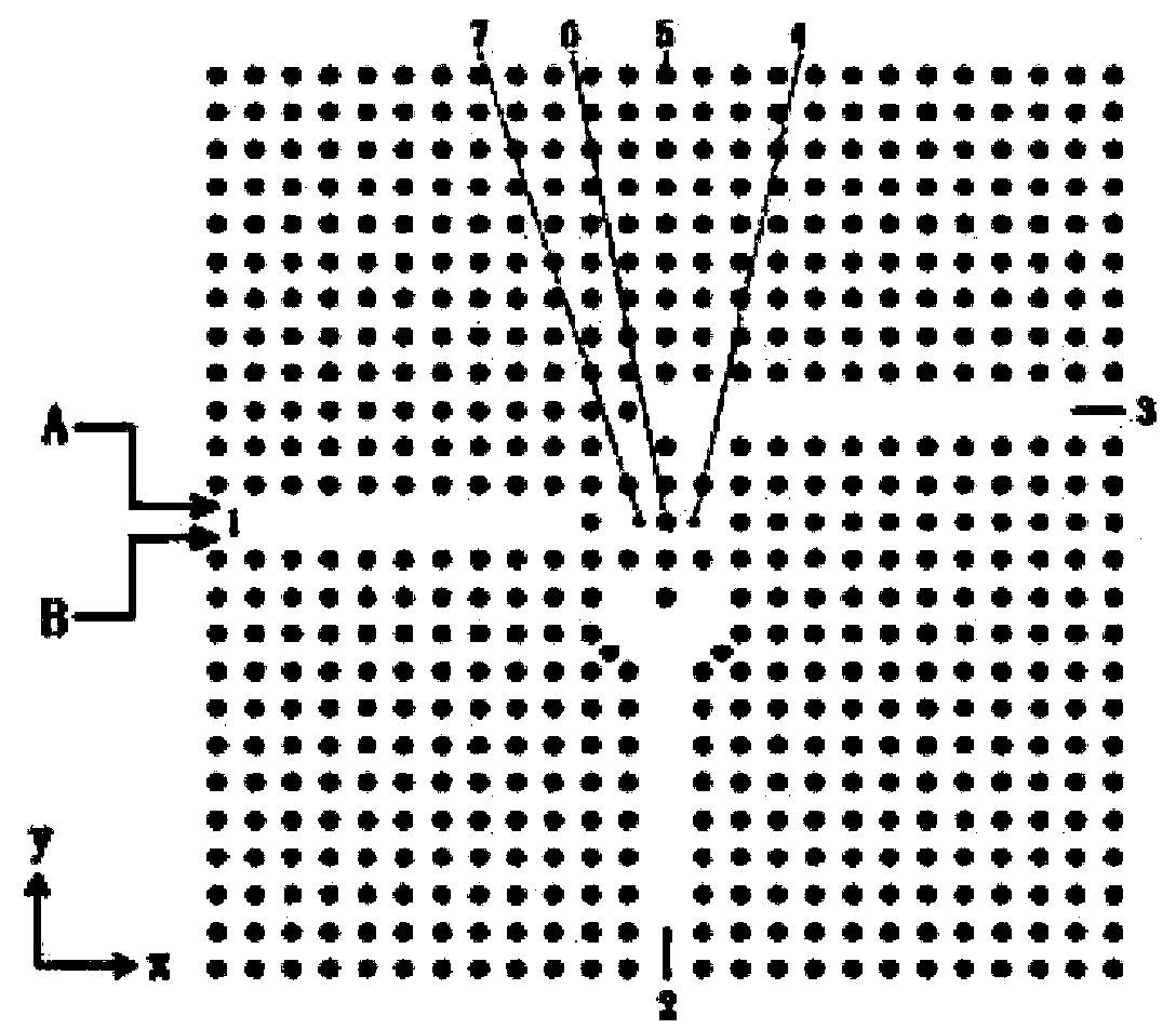
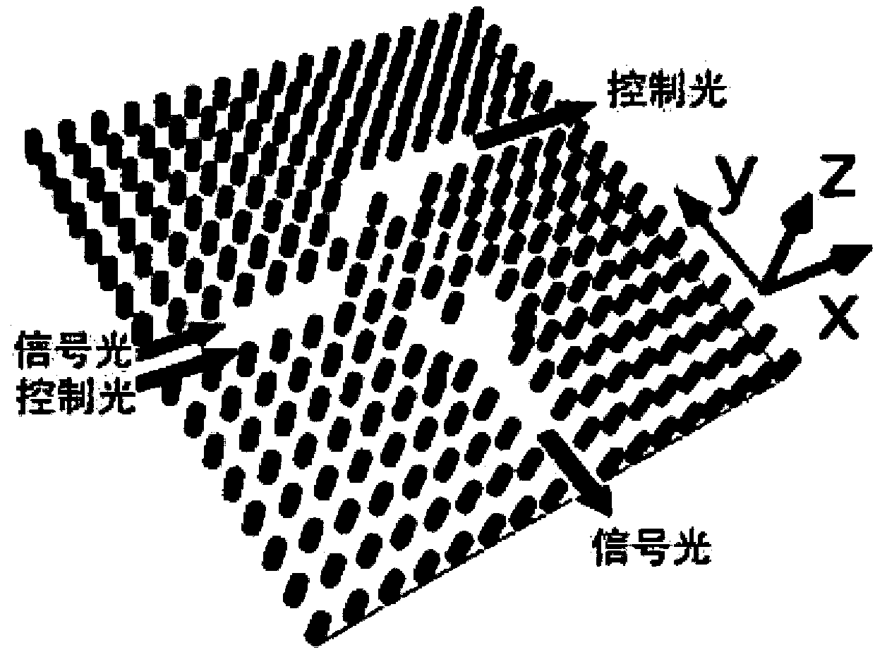
[0041] refer to figure 1 As shown, when the lattice constant a=1 μm, the radius of the circular high-refractive index linear dielectric column 5 and the central dielectric column 6 is 0.2 μm; the movable dielectric column 4 and dielectric column 7 in the two symmetrical resonant cavities in the center of the structure The radius of each is 0.1 μm; let the coordinates of the dielectric column 4 and the dielectric column 7 when the signal light or control light of P0 power is input are (0.6, 0) and (-0.6, 0); set the dielectric column 4 and the dielectric column 7 The coordinates when the signal light of P0 power and the control light of P1 power are input at the same time are (0.7, 0) and (-0.7, 0); the signal light A is input from input port 1 to the signal light and control light input waveguide Middle; control light B is input from input port 1 to signal light and control light input waveguide; signal light A is sent to output port 2 through signal light output waveguide; co...

Embodiment 2

[0048] refer to figure 1 As shown, when the lattice constant a=0.5704μm, the radius of the circular high refractive index linear dielectric column 5 and the central dielectric column 6 is 0.1141μm; the movable dielectric column 4 and the dielectric column in the two symmetrical resonant cavities in the center of the structure The radii of 7 are both 0.057 μm; the coordinates of the dielectric column 4 and the dielectric column 7 when the signal light or control light of P0 power is input are respectively (0.3422, 0) and (-0.3422, 0); the dielectric column 4 and the medium The coordinates of column 7 when the signal light of P0 power and the control light of P1 power are input at the same time are (0.3993, 0) and (-0.3993, 0); signal light A is input from input port 1 to signal light and control light input In the waveguide; the control light B is input from the input port 1 to the signal light and the control light input waveguide; the signal light is output from the output po...


PUM

PropertyMeasurementUnit
Radiusaaaaaaaaaa
Radiusaaaaaaaaaa

Abstract

The invention discloses a photonic crystal all-optical tunable filter. The tunable filter is of a two-dimension photonic crystal structure and comprises three ports, a signal light and controlling light input waveguide, a signal light output waveguide and a controlling light output waveguide. Two photonic crystal defect cavities are symmetrically formed in the intersection position of the three waveguides, and a movable dielectric cylinder is arranged in each photonic crystal defect cavity. Several dielectric cylinders are respectively removed from the upper portion and the lower portion of each photonic crystal defect cavity, and the upper portions of the photonic crystal defect cavities and the controlling light output waveguide form an odd mode output structure, and the lower portions of the photonic crystal defect cavities and the signal light output waveguide form an even mode output structure. The photonic crystal all-optical tunable filter is simple in structure, high in response speed, high in anti-interference performance and easy to integrate with other optical logic elements.

Description

technical field [0001] The invention relates to two-dimensional photonic crystals and photomechanical force effects Background technique [0002] In 1987, E. Yablonovitch of Bell Laboratories in the United States was discussing how to suppress spontaneous emission and S. John of Princeton University was discussing the photonic region and independently proposed the concept of photonic crystals (Photonic Crystals). A photonic crystal is a material structure in which dielectric materials are periodically arranged in space, and is usually an artificial crystal composed of two or more materials with different dielectric constants. [0003] With the introduction and in-depth research of photonic crystals, people can more flexibly and effectively control the movement of photons in photonic crystal materials. In combination with traditional semiconductor technology and integrated circuit technology, people are making rapid progress towards all-optical processing through the design ...

Claims


Application Information

Patent Timeline
IPC IPC(8): G02B6/122
CPCG02B6/1225G02B6/29395G02B6/359
Inventor 欧阳征标余铨强郑耀贤
Owner SHENZHEN UNIV
Why Eureka
Try Eureka