Ultraviolet single-wavelength MSM photoelectric detector based on two-dimensional crystal lattices

A photodetector and single-wavelength technology, applied in circuits, electrical components, semiconductor devices, etc., can solve the problems of immature thin film epitaxial growth technology, high film defect density, and lack of resolution and detection capabilities of ultraviolet light signals

Active Publication Date: 2013-12-25
XIAMEN UNIV
View PDF2 Cites 8 Cited by
  • Summary
  • Abstract
  • Description
  • Claims
  • Application Information

AI Technical Summary

Problems solved by technology

However, conventional Al x Ga 1-x N-based semiconductor ultraviolet photodetectors respond to ultraviolet light with a wavelength shorter than the absorption band edge (A.Knigge, et.al, "AlGaN photodetectors for the UV-C spectral region on planar and epitaxial laterally overgrown AlN / sapphire templates, "Physica Status Solidi(C), vol.10, no.3, pp.294-297, Mar.2013.; F.Xie, et.al, "Large-area solar-blind AlGaN-based MSM photodetectors with ultra- low dark current, "Electronics Letters, vol.47, no.16, p.930, 2011.) and the ultraviolet light signal of a specific wavelength within the response range has no resolution and detection capabilities, which restricts the application of semiconductor ultraviolet photodetectors ; on the other hand, due to the high Al composition Al x Ga 1-x N (x>0.4) film epitaxial growth technology is not yet mature, and the grown film has a high defect density (Y.-L.Tsai, et.al, "Observation of compositional pulling phenomenon in Al x Ga 1-x N(0.4x Ga 1-x Development of N-based ultraviolet photodetectors towards short wavelength

Method used


Image

  • Ultraviolet single-wavelength MSM photoelectric detector based on two-dimensional crystal lattices
  • Ultraviolet single-wavelength MSM photoelectric detector based on two-dimensional crystal lattices

Examples


Embodiment Construction

[0020] The present invention will be further described below in conjunction with the accompanying drawings and embodiments.

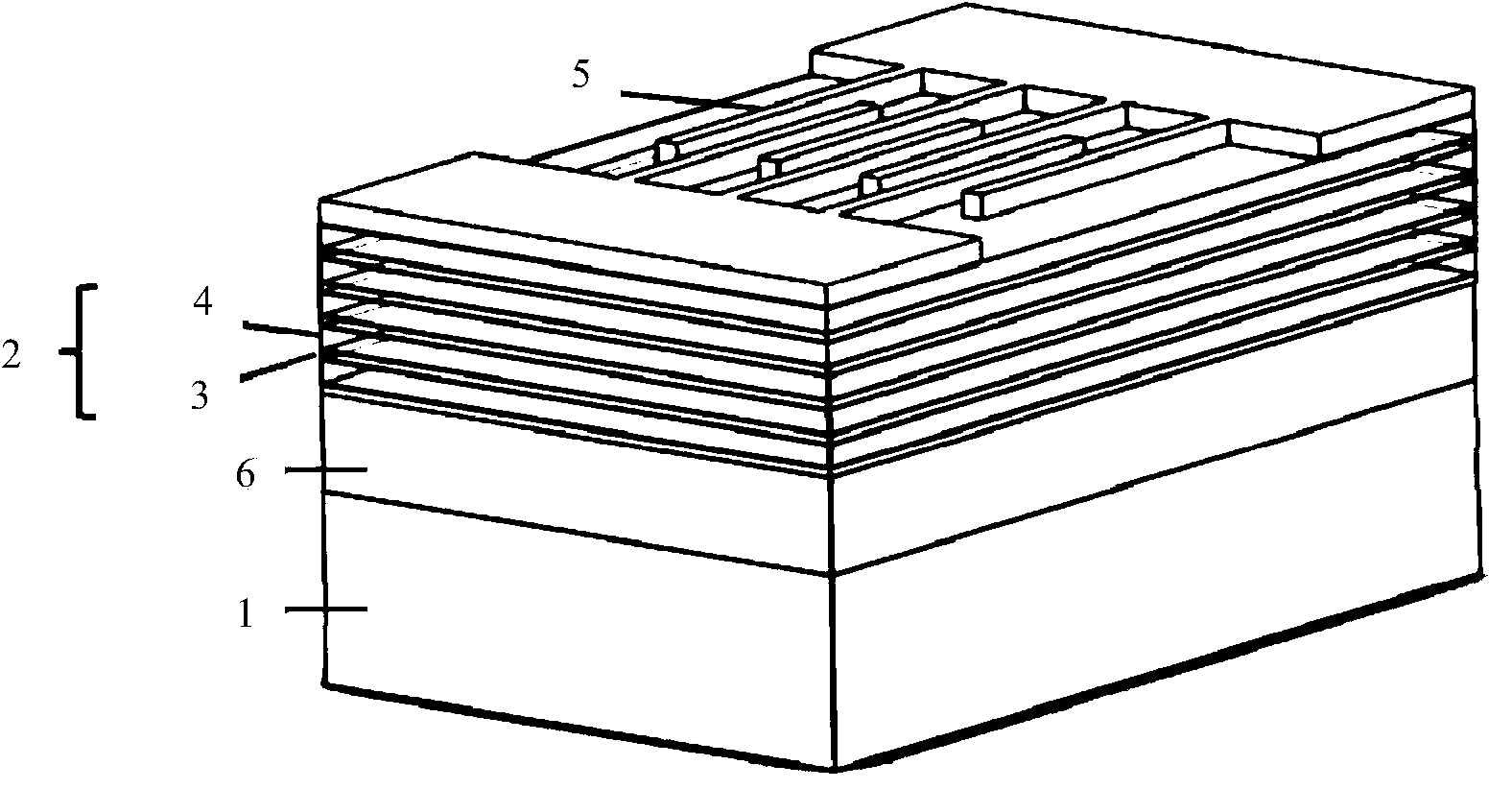
[0021] The present invention includes a substrate 1, a buffer layer 6, a plurality of two-dimensional lattices 2 (consisting of a first dielectric film layer 3 and a second dielectric film layer 4) with quantum energy levels alternately growing on the substrate 1, and Metal interdigitated electrodes 5 .

[0022] The substrate 1 is a sapphire (heterogeneous substrate), and an AlN matrix layer is epitaxially grown on the surface of the sapphire, and the thickness of the AlN matrix layer can be 100 nm to 1 μm. The AlN matrix layer serves as the buffer layer 6 . The AlN matrix layer can release stress, reduce the lattice mismatch between the sapphire substrate and the two-dimensional lattice material, and ensure good quality of crystal growth. The two-dimensional lattice 2 of each alternate growth period is formed by the first dielectric film layer 3 and ...


PUM


Abstract

The invention discloses an ultraviolet single-wavelength MSM photoelectric detector, and belongs to the technical field of semiconductor photoelectric devices. The ultraviolet single-wavelength MSM photoelectric detector based on two-dimensional crystal lattices uses the quantum restriction effect to achieve the adjustable single wavelength and can develop the advantage of high quantum level state density more easily. The ultraviolet single-wavelength MSM photoelectric detector comprises a substrate, the two-dimensional crystal lattices with the quantum level and a metal interdigital electrode. The two-dimensional crystal lattices grow on the substrate alternatively, and the number of the alternative growth periods is at least 20. Each two-dimensional crystal lattice in each alternative growth period is composed of a first dielectric film layer and a second dielectric film layer, wherein the forbidden band of the first dielectric film layer is arranged in the forbidden band of the second dielectric film layer and forms a semiconductor I-class superlattice, the first dielectric film is used as a potential well, and the second dielectric film is used as a potential barrier; the Schottky contact is formed between the metal interdigital electrode and the two-dimensional crystal lattices.

Description

technical field [0001] The invention belongs to the technical field of semiconductor optoelectronic devices, and relates to a metal-semiconductor-metal (MSM) photodetector, in particular to an ultraviolet single-wavelength MSM photodetector based on a two-dimensional lattice. Background technique [0002] Ultraviolet detection technology has broad application prospects in military and civilian fields. In the military, it can be used for missile guidance, missile early warning, ultraviolet communication, etc.; in the civilian field, it can be used in flame detection, environmental monitoring, biomedical analysis, etc., and has become one of the international research hotspots of photoelectric detection technology in recent years. The structures of common solid-state detectors in UV detection technology include metal-semiconductor-metal (MSM), photoconductive, and p-i-n-type structures. In contrast, the MSM structure is favored due to its small capacitance, planarity, no dopi...

Claims


Application Information

Patent Timeline
Patent Type & Authority Applications(China)
IPC IPC(8): H01L31/101H01L31/0248
Inventor 康俊勇高娜黄凯陈雪林伟李书平陈航洋杨旭李金钗
Owner XIAMEN UNIV
Why Eureka
Try Eureka