Method for preparing reflecting film, solar cell panel and its crystalline silicon wafer

A technology of crystalline silicon wafers and reflective films, applied in the field of solar cells, can solve problems such as reducing the solar light efficiency of crystalline silicon wafers

Active Publication Date: 2013-12-25
RENESOLA JIANGSU LTD
View PDF3 Cites 2 Cited by
  • Summary
  • Abstract
  • Description
  • Claims
  • Application Information

AI Technical Summary

Problems solved by technology

In order to reduce the cost of raw materials, people began to use thinner crystalline silicon wafers. For thinner crystalline silicon wafers, only an all-aluminum back field is set on the back surface, which not only limits the further improvement of photoelectric conversion efficiency, but also because The crystalline silicon wafer itself is thin, so that sunlight is easily transmitted from the back of the crystalline silicon wafer, which reduces the efficiency of the crystalline silicon wafer to absorb sunlight

Method used


Image

  • Method for preparing reflecting film, solar cell panel and its crystalline silicon wafer
  • Method for preparing reflecting film, solar cell panel and its crystalline silicon wafer

Examples


preparation example Construction

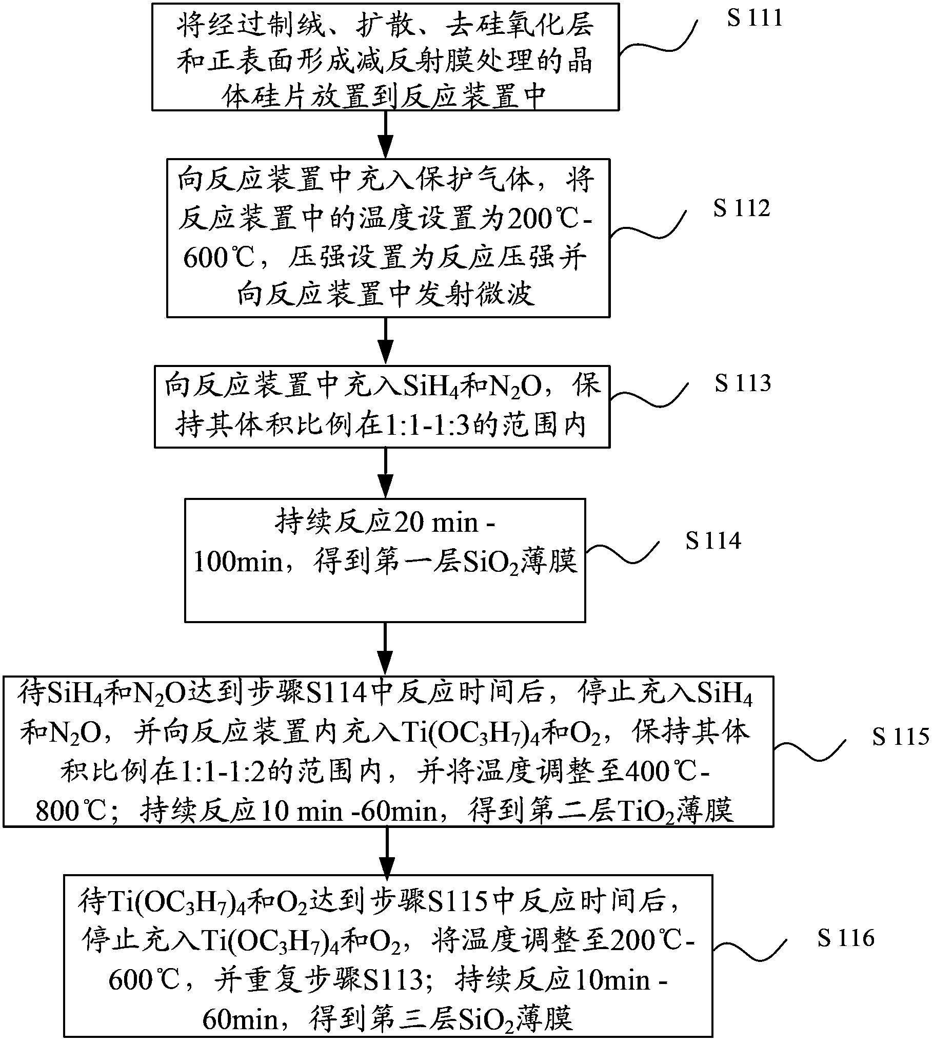
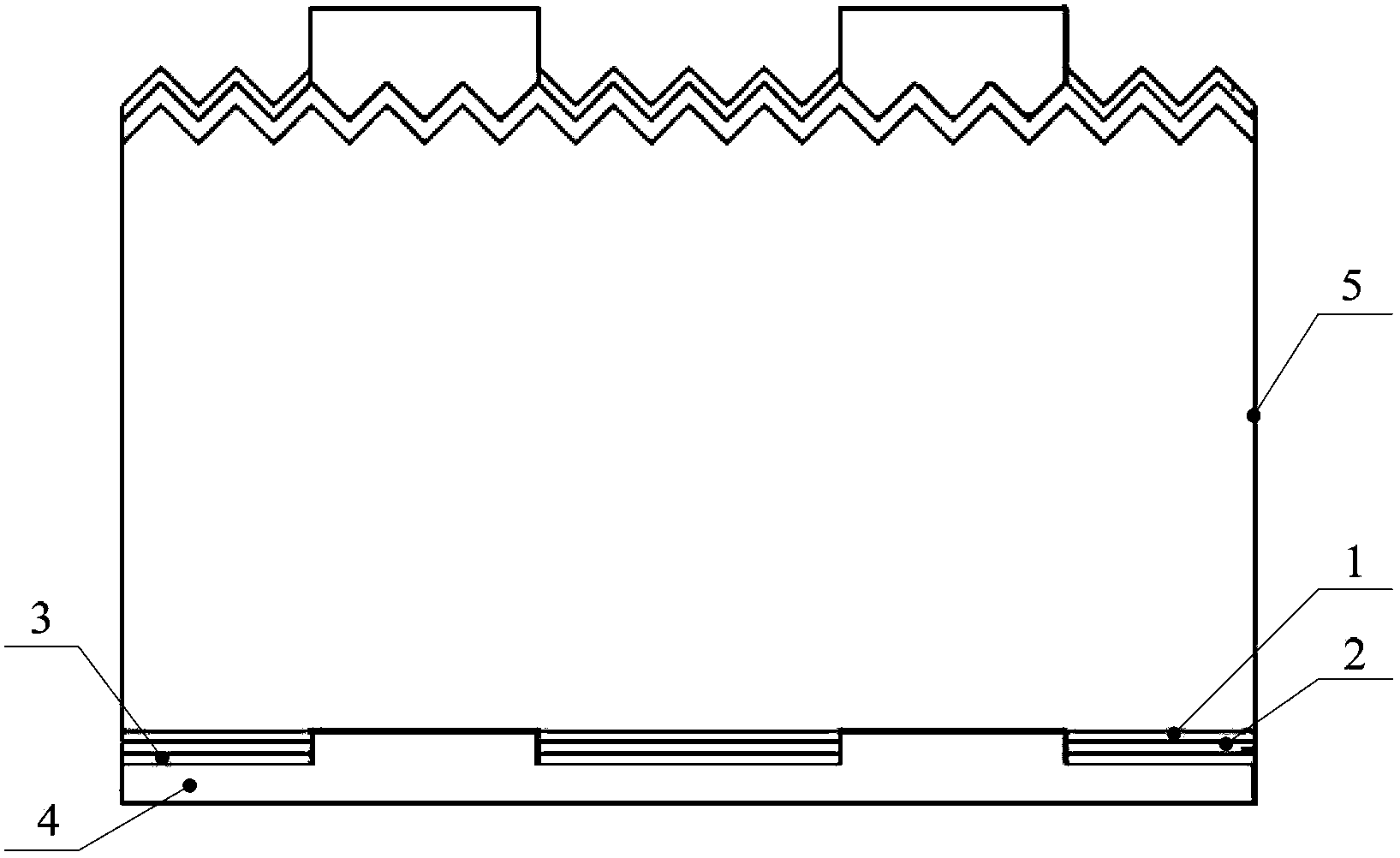
[0035] The method for preparing a reflective film provided in the embodiment of the present invention is used to prepare a reflective film on the back surface of a crystalline silicon wafer 5, comprising the following steps:

[0036] S111 placing the crystalline silicon wafer 5 treated with texturing, diffusion, silicon oxide layer removal and anti-reflection film formation on the front surface into the reaction device;

[0037] S112 filling the reaction device with protective gas, setting the temperature in the reaction device to 200°C-600°C, setting the pressure to the reaction pressure and emitting microwaves into the reaction device;

[0038] S113 Fill SiH into the reaction device 4 and N 2 O, keep its volume ratio in the scope of 1:1-1:3;

[0039] S114 continues to react for 20min-100min to obtain the first layer of SiO 2 film1;

[0040] S115 to be SiH 4 and N 2 After O reaches the reaction time in step S114, stop charging SiH 4 and N 2 O, and fill the reactor wit...

Embodiment 1

[0052] Place the crystalline silicon wafer 5 through texturing, diffusion, silicon oxide layer removal and anti-reflection film formation on the front surface in the quartz furnace tube, and fill it with N 2 As a protective gas, the temperature in the quartz furnace tube is raised to 200°C, the pressure is raised to 0.02mbar, microwaves with a power of 2500W are emitted into the quartz furnace tube, and the SiH 4 and N 2 O is continuously filled into the quartz furnace tube at a volume ratio of 1:1, so that SiH 4 and N 2 O takes place chemical reaction, and reaction time continues 20min, to deposit the first layer SiO on the back surface of crystalline silicon wafer 5 2 Film 1; after the above process is completed, the temperature in the quartz furnace tube is raised to 400°C, the pressure and microwave power are still 0.02mbar and 2500W respectively, and the quartz furnace tube is filled with Ti(OC 3 h 7 ) 4 and O 2 , the reaction time is maintained for 20min, and then ...

Embodiment 2

[0055] Place the crystalline silicon chip 5 with thick anti-reflection film formed on the front surface through texturing, diffusion, silicon oxide layer removal and anti-reflection film thickness into the quartz furnace tube, and fill it with N 2 As a protective gas, the temperature in the quartz furnace tube is raised to 300°C, the pressure is raised to 0.065mbar, microwaves with a power of 2750W are emitted into the quartz furnace tube, and the SiH 4 and N 2 O is continuously filled into the quartz furnace tube at a volume ratio of 1:1.5, so that SiH 4 and N 2 A chemical reaction occurs in O, and the reaction time lasts for 40 minutes to deposit the first layer of SiO on the back surface of the crystalline silicon wafer 5 2 Film 1; after the above process is completed, the temperature in the quartz furnace tube is raised to 500°C, the pressure and microwave power are still 0.065mbar and 2750W respectively, and Ti(OC 3 h 7 ) 4 and O 2 , the reaction time is maintained ...


PUM


Abstract

The invention provides a method for preparing a reflecting film. The method comprises the following steps: protective gas is filled into reaction equipment, pressurization is carried out and microwave is transmitted, the temperature in the reaction equipment is adjusted to a first temperature, silane and nitrous oxide are filled according to the volume ratio of 1:1-1:3; reaction lasts for 20-100 min so as to obtain a first layer of silicon dioxide thin-film; after 20-100 min, filling of silane and nitrous oxide is stopped, tetraisopropyltitanium and oxygen are filled according to the volume ratio of 1:1-1:2, and the temperature is adjusted to a second temperature; reaction lasts for 10-60 min so as to obtain a second layer of titanium dioxide thin-film; after reaction between tetraisopropyltitanium and oxygen, filling of tetraisopropyltitanium and oxygen is stopped, the temperature is adjusted to the first temperature, and silane and nitrous oxide are filled; and reaction lasts for 10-60 min so as to obtain a third layer of silicon dioxide thin-film. According to the invention, transmissivity of sunshine is reduced remarkably. The invention also provides a crystalline silicon wafer of the reflecting film obtained by the above method and a solar cell panel with the crystalline silicon wafer.

Description

technical field [0001] The present invention relates to the technical field of solar cells, and more specifically, relates to a method for preparing a reflective film. The present invention also relates to a crystalline silicon wafer whose back surface is provided with a reflective film prepared by the above-mentioned method, and a crystalline silicon wafer having the above-mentioned crystalline silicon slices of solar panels. Background technique [0002] With the continuous deepening of research on solar cells, the focus of the development of crystalline silicon solar cells is high efficiency and low cost. [0003] The crystalline silicon wafers of conventional solar panels adopt an all-aluminum back field structure printed on the back. The specific production process is: the crystalline silicon wafers are textured, diffused, and PSG (Phospho Silicate Glass, silicon oxide layer containing higher phosphorus concentration is removed. It is called phosphosilicate glass) and ...

Claims


Application Information

Patent Timeline
Patent Type & Authority Applications(China)
IPC IPC(8): H01L31/18H01L31/0216H01L31/052
CPCY02E10/52Y02P70/50
Inventor 徐世贵王立建
Owner RENESOLA JIANGSU LTD
Why Eureka
Try Eureka