

Low-k intermetallic dielectric (Low-k IMD) layer etching method
An inter-metal dielectric layer, low dielectric constant technology, applied in circuits, electrical components, semiconductor/solid-state device manufacturing, etc., can solve problems such as Low-kIMD damage, and achieve the effect of eliminating damage
- Summary
- Abstract
- Description
- Claims
- Application Information
AI Technical Summary
Problems solved by technology
Method used
Image

Examples
specific Embodiment 1
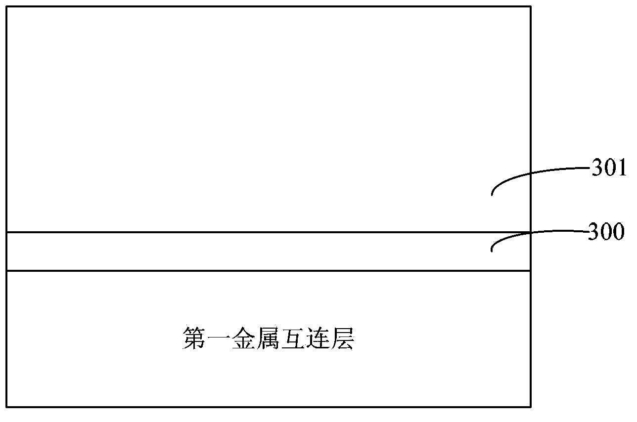
[0047] combine Figure 9~15 Description such as Figure 8 The specific steps of etching through holes and grooves in the shown embodiment of the present invention-Low-k IMD layer are as follows:
[0048] Step 801, Figure 9 It is a schematic diagram of the cross-sectional structure of the step 801 of etching vias and trenches in the Low-k IMD layer of the present invention, as Figure 9 As shown, an etch stop layer 300 and a Low-k intermetal dielectric (IMD) layer 301 are sequentially deposited on the first metal interconnection layer; in this step, a wafer is provided, and the wafer has the first metal interconnection layer ; In this embodiment, only the first metal interconnection layer is taken as an example to illustrate the metal interconnection method of the present invention, and the first metal interconnection layer shown can be any metal interconnection layer in practical applications. The material of the etching stop layer 300 is silicon carbonitride (SiCN), and t...
specific Embodiment 2
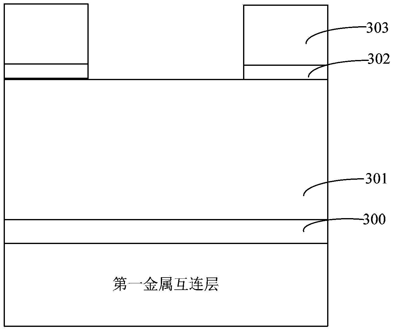
[0071] combine Figure 17~19 Description such as Figure 16 The specific steps of etching through holes and trenches in the Low-k IMD layer of the second embodiment of the present invention are shown, wherein, steps 1001 to 1004 of the second embodiment of the present invention and steps 801 to 804 of the first embodiment of the present invention Same, no more details.
[0072] Step 1005, Figure 17 It is a schematic cross-sectional structure diagram of the manufacturing step 1005 of etching via holes and trenches in the Low-k IMD of the second embodiment of the present invention, as Figure 17 As shown, the Low-k intermetallic dielectric layer 301 is etched to form trenches and via holes with the hard mask as a shield, and stop on the etching stop layer;
[0073] In this step, the method for etching the Low-k intermetallic dielectric layer 301 is dry etching, and the end point detection method is used to control the stop of etching, and the etching stop layer 300 is used a...
PUM
| Property | Measurement | Unit |
|---|---|---|
| thickness | aaaaa | aaaaa |
Abstract
Description
Claims
Application Information