LED chip and processing technology thereof

An LED chip and processing technology technology, applied in electrical components, circuits, semiconductor devices, etc., can solve the problems of affecting the thermal stability of the chip, the area cannot emit light, and the effective light-emitting area of ​​the die is reduced, so as to improve the brightness and light extraction efficiency, The effect of improving brightness and luminous efficiency, and increasing the effective luminous area

Inactive Publication Date: 2014-01-15
YANGZHOU ZHONGKE SEMICON LIGHTING
View PDF5 Cites 19 Cited by
  • Summary
  • Abstract
  • Description
  • Claims
  • Application Information

AI Technical Summary

Problems solved by technology

This method causes the P-type nitride and quantum wells on one side of the die to be destroyed in a large area, making this area unable to emit light
This reduces the effective light-emitting area of ​​the die, which greatly affects the brightness of the die. Taking a die with a size of 10mil×23mil as an example, in order to ensure the reliability of the package, the area of ​​the electrode pad is generally twice the diameter of the gold wire. , so the diameter of the pad is usually 80 μm, that is, the light-emitting area lost by the N-electrode pad accounts for about 7% of the effective light-emitting area of ​​the die
At the same time, the material used for the PN pad of the existing LED chip is a metal material with poor reflectivity. These materials have a large absorption of blue-green light, which affects the light extraction efficiency of the LED chip and also affects the thermal stability of the chip.
In addition, in the process of chip packaging, using the existing technology will inevitably cause obvious height differences between the PN electrode pads. If the pressure of the P and N pads is not properly controlled, it is easy to damage the chip surface and increase the leakage of the die. even dead lights

Method used


Image

  • LED chip and processing technology thereof

Examples


Embodiment Construction

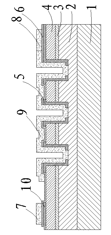
[0022] One, such as figure 1 As shown, the processing technology:

[0023] 1. Preparation of epitaxial substrate: N-type nitride layer 2, quantum well layer 3 and P-type nitride layer 4 are sequentially fabricated on substrate layer 1 such as sapphire (other materials used in the industry can also be used).

[0024] 2. Etching part of the P-type nitride layer 4 on the epitaxial wafer substrate, removing the P-type nitride layer 4 and the quantum well layer 3 in a part of the epitaxial wafer substrate, and exposing the N-type nitride layer 2 . The etching method can be inductively coupled plasma etching method, or electron cyclotron resonance etching method, or reactive ion etching method. The etching depth and process conditions are the same as the conventional LED manufacturing process.

[0025] 3. Make a current blocking layer under the designed P-type electrode pad area: use the PECVD growth method to grow an insulating material with a thickness of 2000? on the substrate ...


PUM


Abstract

The invention relates to an LED chip and a processing technology thereof, and belongs to the technical field of manufacturing of photoelectron devices. The technology comprises the following steps: a P-type nitride layer on an epitaxial wafer substrate is etched to expose an N-type nitride layer; a current blocking layer is manufactured under a P-type electrode bonding pad area, an insulating substance under the P-type electrode bonding pad area, an insulating substance in direct contact with an N-type electrode bonding pad, and an expanding electrode and the P-type nitride layer, and an insulating substance on the side walls of a quantum well and P-type nitride are reserved through etching; an ITO film deposits on the surface of the substrate, a current expanding layer and alloy are manufactured through photoetching, a metal layer is formed on the surface of the substrate through vapor deposition, and after a part of the metal layer is stripped, a P-type electrode bonding pad, an N-type electrode bonding pad and an N metal expanding electrode are formed. Both the P-type electrode bonding pad and the N-type electrode bonding pad of the product are positioned on a P-type light-emitting surface and are the same in height; a part or all of the N metal expanding electrode is in direct contact with the N-type nitride layer. The invention has the advantages that the routing is convenient, the light-emitting efficiency and the brightness of the LED chip on the nitride substrate can be improved.

Description

technical field [0001] The invention belongs to the technical field of manufacturing semiconductor optoelectronic devices, and in particular relates to a manufacturing technology of an N electrode pad and a metal extended electrode in the manufacturing process of a nitride substrate light-emitting diode (LED). Background technique [0002] In recent years, nitride-based LED chip technology has developed by leaps and bounds, and is widely used in many fields such as display screens, backlights, and lighting. At the same time, these applications have also raised higher and higher requirements for the brightness and luminous efficiency of LED chips. Require. With the development of nitride-based LED epitaxial growth technology and multiple quantum well structures, the internal quantum efficiency of nitride-based LEDs has been greatly improved, but the external quantum efficiency of LED chips has not been well improved. How to pass Adjusting the chip structure to improve the qu...

Claims


Application Information

Patent Timeline
Patent Type & Authority Applications(China)
IPC IPC(8): H01L33/38H01L33/00
CPCH01L33/36H01L33/385
Inventor 冯亚萍张溢金豫浙李佳佳李志聪孙一军王国宏
Owner YANGZHOU ZHONGKE SEMICON LIGHTING
Why Eureka
Try Eureka