Semiconductor device production method and semiconductor device

A manufacturing method and semiconductor technology, applied in the direction of semiconductor/solid-state device manufacturing, semiconductor devices, semiconductor/solid-state device components, etc., can solve the problems of increased reverse leakage, increased reverse leakage, and inability to add, etc. Excellent insulation, low reverse leakage current, and improved insulation effects

Active Publication Date: 2014-01-15
SHINDENGEN ELECTRIC MFG CO LTD
View PDF8 Cites 14 Cited by
  • Summary
  • Abstract
  • Description
  • Claims
  • Application Information

AI Technical Summary

Problems solved by technology

[0023] However, "glass materials mainly composed of lead silicate" contain lead, which has a large burden on the environment, so it is expected that the use of "glass materials mainly composed of lead silicate" will be banned in the near future
[0024] Therefore, although it is also conceivable to use lead-free glass materials to form the glass layer for passivation, but satisfy (a) can be fired at an appropriate temperature; (b) have chemical resistance to the chemicals used in the process ; (c) having a linear expansion coefficient close to that of silicon (in particular, an average linear expansion coefficient at 50°C to 550°C close to that of silicon) in order to prevent warping of wafers in the process; and (d ) have excellent insulating properties and all these conditions are difficult, and the method of forming the glass layer for passivation using a lead-free glass material has not yet been applied to mass production of power (power) semiconductor devices This is also true in the process
[0025] In addition, studies by the inventors of the present invention have clarified that when a glass layer for passivation is formed using a lead-free glass material, the process of forming a glass layer by firing a layer made of a glass composite Among them, depending on the composition of the glass layer and firing conditions, there is a problem that bubbles are easily generated from the interface between the semiconductor substrate and the glass layer.
In order to solve such problems, it is necessary to add components that have a degassing effect (such as nickel oxide, zirconium oxide, etc.), but depending on the combination of glass components, there may be cases where it cannot be added, so it is not necessary. Be applicable
[0026] In addition, through the research of the inventors of the present invention, it has been clarified that when the glass layer for passivation is formed using a lead-free glass material, depending on the composition of the glass layer and the firing conditions (the composition of the glass: When highly SiO-containing 2 When the glass is used, firing conditions: in a short time), there will be a problem of increased reverse leakage (leak) flow
In other words, it was clarified that if firing for a long time (for example: 3 hours) is necessary, there will be a problem that the reverse leakage current will increase

Method used


Image

  • Semiconductor device production method and semiconductor device
  • Semiconductor device production method and semiconductor device
  • Semiconductor device production method and semiconductor device

Examples


Embodiment approach 1

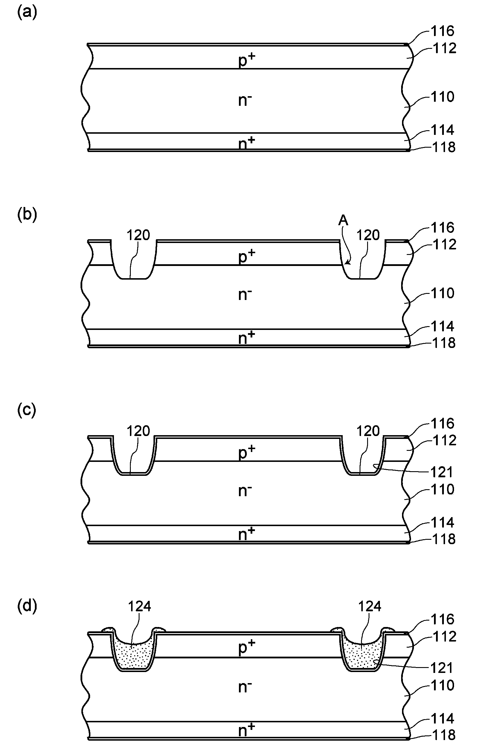
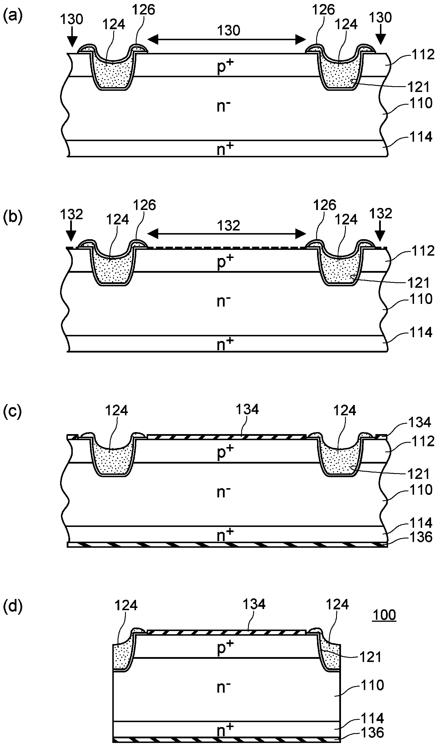
[0081] The method for manufacturing a semiconductor device according to Embodiment 1 includes in order: a first step of preparing a semiconductor element having a pn junction exposed portion; a second step of forming an insulating layer covering the pn junction exposed portion; and a third step of After forming a layer made of a glass compound for protecting a semiconductor junction on the insulating layer, the layer made of the glass compound for protecting a semiconductor junction is fired to form a glass layer on the insulating layer. In the method of manufacturing a semiconductor device according to Embodiment 1, a mesa-type pn diode is manufactured as a semiconductor device.

[0082] figure 1 and figure 2 It is a figure for demonstrating the manufacturing method of the semiconductor device of Embodiment 1. figure 1 (a) ~ figure 1 (d) and figure 2 (a) ~ figure 2 (d) is a diagram of each process.

[0083] like figure 1 and figure 2 As shown, the manufacturin...

Embodiment approach 2

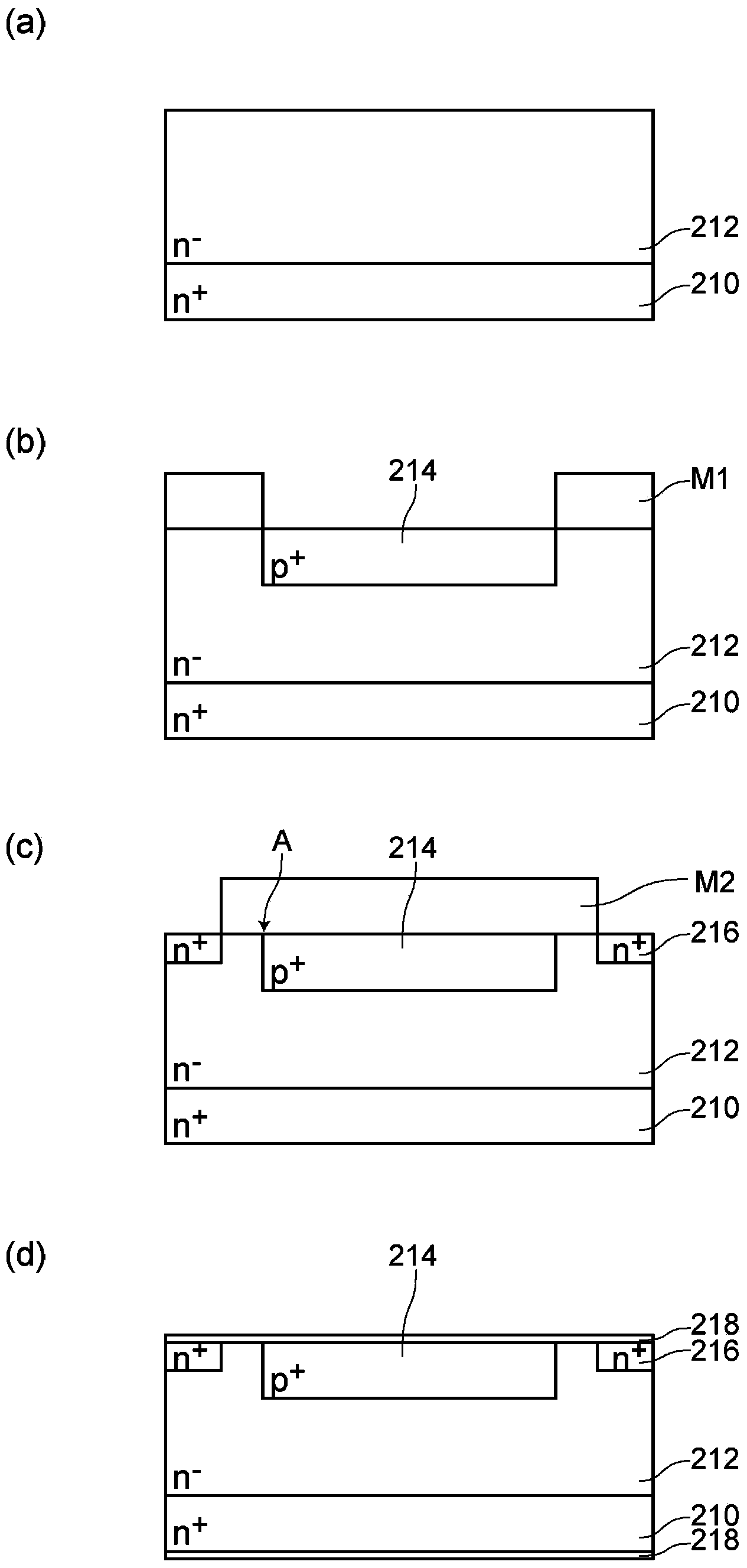
[0125] The method of manufacturing a semiconductor device according to Embodiment 2, like the method of manufacturing a semiconductor device according to Embodiment 1, sequentially includes the first step of preparing a silicon semiconductor element having a pn junction exposed portion; the second step, forming an insulating layer covering the exposed portion of the pn junction; and a third step of forming a layer made of a glass compound for protecting a semiconductor junction on the insulating layer, and then firing the layer made of a glass compound for protecting a semiconductor junction. A method of manufacturing a semiconductor device in which a glass layer is formed on an insulating layer. However, in the method of manufacturing a semiconductor device according to Embodiment 2, a difference from the method of manufacturing a semiconductor device according to Embodiment 1 is that a planar type pn diode is manufactured as a semiconductor device.

[0126] image 3 with ...

Embodiment approach 3

[0154] The manufacturing method of the semiconductor device related to the third embodiment, like the manufacturing method of the semiconductor device related to the first embodiment, includes the first step in sequence, preparing a semiconductor element having a pn junction exposed portion where the pn junction is exposed; the second step, forming a covering The insulating layer of the exposed part of the pn junction; and the third step, after forming a layer made of the glass compound for semiconductor junction protection on the insulating layer, by firing the layer made of the glass compound for semiconductor junction protection, on the insulating layer A method of manufacturing a semiconductor device on which a glass layer is formed. In addition, as the glass compound for protecting a semiconductor joint, a glass compound for protecting a semiconductor joint is used, which is composed of glass fine particles obtained from a melt obtained by melting a raw material containing...


PUM

PropertyMeasurementUnit
thicknessaaaaaaaaaa
thicknessaaaaaaaaaa
thicknessaaaaaaaaaa

Abstract

A semiconductor device production method including, in order: a first step in which a semiconductor element having a pn junction-exposed section is prepared; a second step in which an insulation layer is formed so as to cover the pn junction-exposed section; and a third step in which a layer comprising a glass composition for semiconductor junction protection is formed upon the insulation layer, and then a glass layer is formed upon the insulation layer by sintering the layer comprising the glass composition for semiconductor junction protection. The glass composition for semiconductor junction protection comprises glass fine particles prepared from a melt obtained by melting a raw material containing at least two alkali earth metal oxides from among at least SiO2, Al2O3, B2O3, ZnO, CaO, MgO, and BaO, and not substantially containing Pb, As, Sb, Li, Na, or K. In addition none of the raw material components are included as fillers. As a result, a semiconductor device having high pressure resistance similar to conventional semiconductor devices can be obtained using a glass material not including lead.

Description

technical field [0001] The present invention relates to a method for manufacturing a semiconductor device and the semiconductor device. Background technique [0002] There is known a method of forming a passivation glass layer covering an exposed portion of a pn junction in the process of manufacturing a mesa semiconductor device (for example, refer to Patent Document 1). [0003] Figure 12 and Figure 13 Shown are diagrams for explaining these conventional methods of manufacturing semiconductor devices. Figure 12 (a) ~ Figure 12 (d) and Figure 13 (a) ~ Figure 13 (d) is a diagram of each process. [0004] like Figure 12 and Figure 13 As shown, the conventional semiconductor device manufacturing method includes sequentially "semiconductor substrate formation step", "trench formation step", "glass layer formation step", "photoresist (photoresist) formation step", "oxide film formation step" removal step", "roughened region formation step", "electrode formation step...

Claims


Application Information

Patent Timeline
Patent Type & Authority Applications(China)
IPC IPC(8): H01L21/316C03C3/093H01L29/74H01L29/78H01L29/861H01L29/868
CPCH01L23/3178H01L29/0619H01L29/66136H01L29/861H01L2924/0002H01L2924/00
Inventor 小笠原淳伊东浩二伊藤一彦六鎗広野
Owner SHINDENGEN ELECTRIC MFG CO LTD
Why Eureka
Try Eureka