Adhesive tape for surface protection of a semiconductor wafer and method of producing a semiconductor wafer using the same

A manufacturing method and semiconductor technology, which can be used in the manufacture of semiconductor/solid-state devices, film/sheet adhesives, adhesives, etc., can solve the problem of radiation curing hindering the embeddedness of the periphery of semiconductor wafers, etc., to prevent wafer damage, restrain Residual glue, the effect of reducing peeling force

Active Publication Date: 2014-01-22
FURUKAWA ELECTRIC CO LTD
View PDF8 Cites 6 Cited by
  • Summary
  • Abstract
  • Description
  • Claims
  • Application Information

AI Technical Summary

Problems solved by technology

[0013] In response to this problem, it is considered that adhesive residue and peeling can be improved by partially thinning the adhesive layer so that it does not follow the bumps, but usually in this method, since a gap is generated between the semiconductor wafer and the adhesive, the Intervention of radiation curing due to oxygen in voids or embedding around the semiconductor wafer becomes a problem

Method used


Image

  • Adhesive tape for surface protection of a semiconductor wafer and method of producing a semiconductor wafer using the same
  • Adhesive tape for surface protection of a semiconductor wafer and method of producing a semiconductor wafer using the same
  • Adhesive tape for surface protection of a semiconductor wafer and method of producing a semiconductor wafer using the same

Examples


Embodiment 1

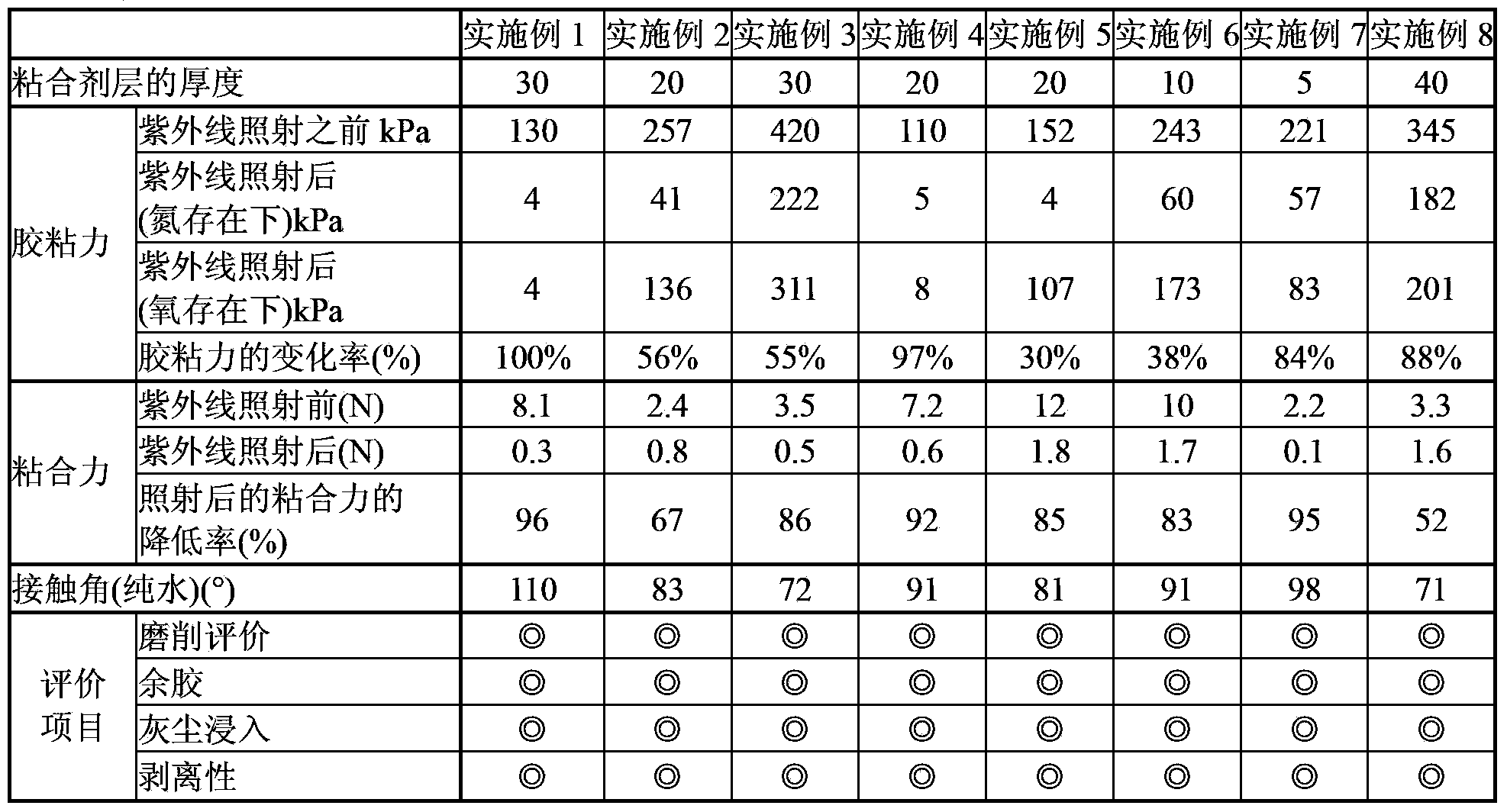
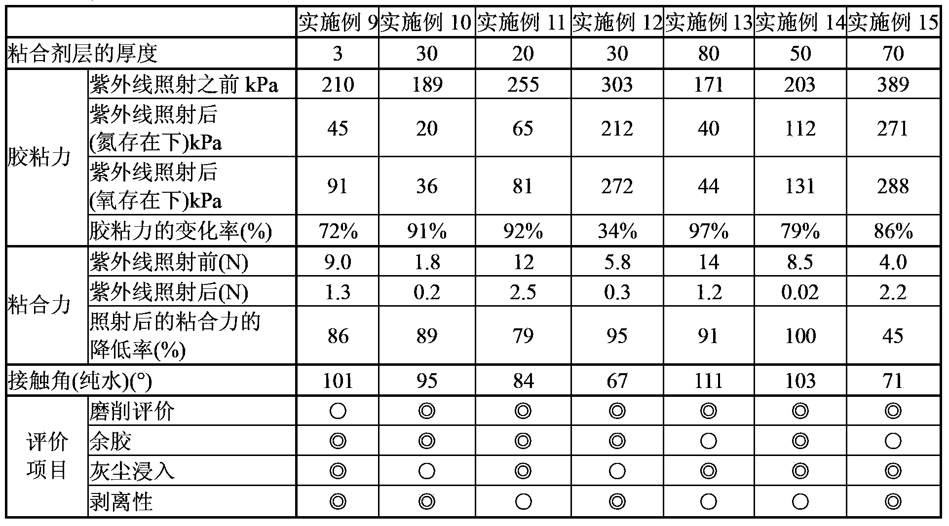
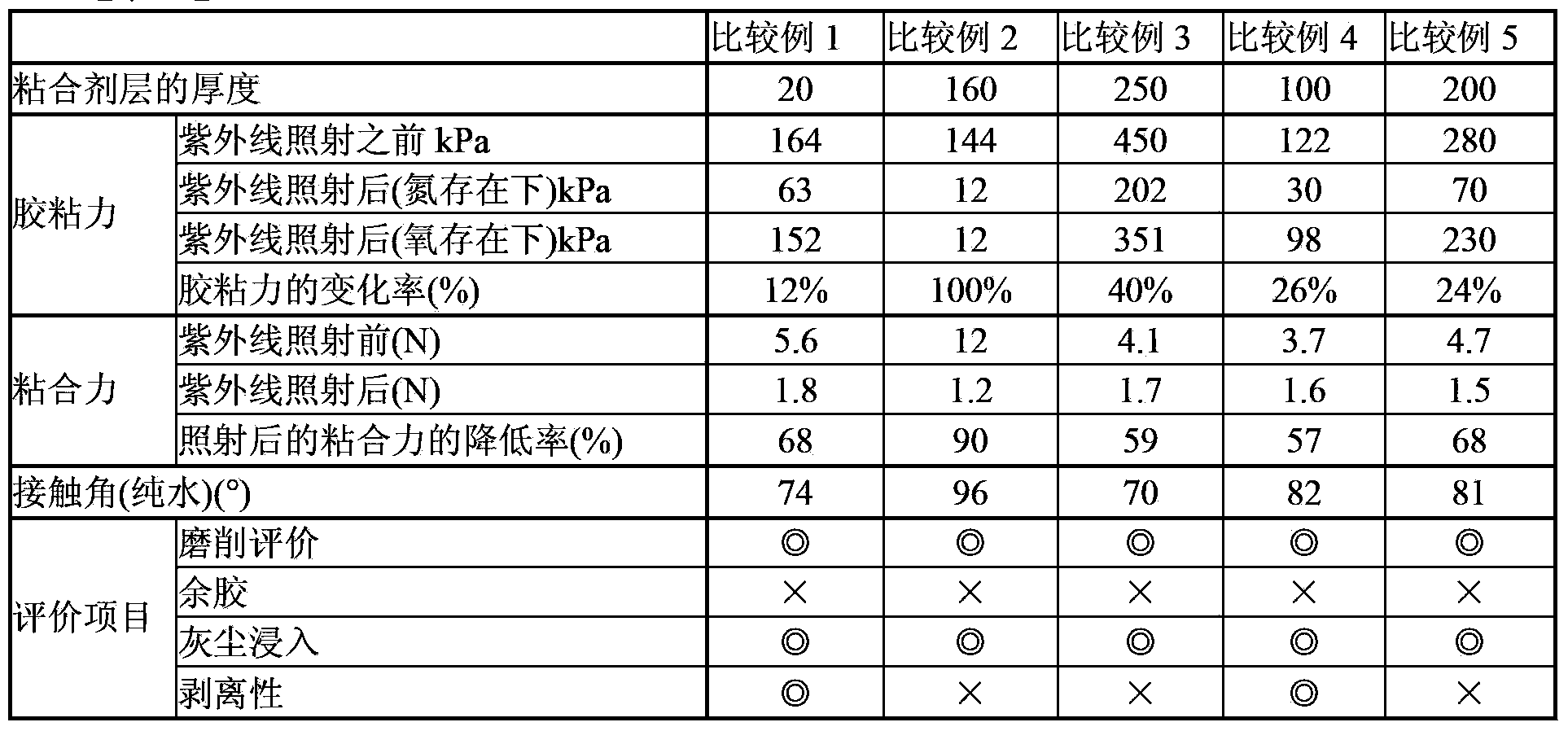
[0122] Polymerize 65 parts by mass of 2-ethylhexyl acrylate, 33 parts by mass of 2-hydroxyethyl acrylate, and 2 parts by mass of methacrylic acid in ethyl acetate, and obtain a copolymer having a weight average molecular weight of 800,000 100 parts by mass, 60 parts by mass of ethyl methacrylate-2-isocyanato was added to obtain an acrylic copolymer. 2 parts by mass of an addition-based isocyanate-based crosslinking agent CORONET L (trade name, manufactured by Nippon Polyurethane Co., Ltd.) and a photopolymerization initiator 4,4'-bis(diethylamino) were mixed with the obtained acrylic copolymer. 2 parts by mass of benzophenone were adjusted with ethyl acetate in order to adjust the viscosity to be easy to apply, and an adhesive composition was obtained.

[0123] On a separation plate of polyethylene terephthalate (PET) with a thickness of 25 μm, the adhesive composition is coated with a film thickness of 30 μm after drying, and after drying, it is pasted on a separation plate w...

Embodiment 2

[0125] Polymerize 72 parts by mass of 2-ethylhexyl acrylate, 26 parts by mass of 2-hydroxyethyl acrylate, and 2 parts by mass of methacrylic acid in ethyl acetate, and obtain a copolymer having a weight average molecular weight of 700,000 100 parts by mass, 20 parts by mass of ethyl methacrylate-2-isocyanato was added to obtain an acrylic copolymer. 1.5 parts by mass of an addition-based isocyanate-based crosslinking agent CORONET L (trade name, manufactured by Nippon Polyurethane Co., Ltd.) and a photopolymerization initiator 4,4'-bis(diethylamino) were mixed with the obtained acrylic copolymer. 2 parts by mass of benzophenone were adjusted with ethyl acetate in order to adjust the viscosity to be easy to apply, and an adhesive composition was obtained.

[0126] On a separation plate of polyethylene terephthalate (PET) with a thickness of 25 μm, the adhesive composition is coated with a film thickness of 20 μm after drying, and after drying, it is pasted on a separation plate...

Embodiment 3

[0128] Polymerize 68 parts by mass of 2-ethylhexyl acrylate, 30 parts by mass of 2-hydroxyethyl acrylate, and 2 parts by mass of methacrylic acid in ethyl acetate, and obtain a copolymer having a weight average molecular weight of 800,000 100 parts by mass, 20 parts by mass of ethyl methacrylate-2-isocyanato was added to obtain an acrylic copolymer. 2 parts by mass of an addition-based isocyanate-based crosslinking agent CORONET L (trade name, manufactured by Nippon Polyurethane Co., Ltd.) and a photopolymerization initiator 4,4'-bis(diethylamino) were mixed with the obtained acrylic copolymer. 2 parts by mass of benzophenone were adjusted with ethyl acetate in order to adjust the viscosity to be easy to apply, and an adhesive composition was obtained.

[0129] On a separation plate of polyethylene terephthalate (PET) with a thickness of 25 μm, the adhesive composition is coated with a film thickness of 30 μm after drying, and after drying, it is pasted on a separation plate w...


PUM

PropertyMeasurementUnit
contact angleaaaaaaaaaa
thicknessaaaaaaaaaa
thicknessaaaaaaaaaa

Abstract

The invention provides an adhesive tape for surface protection of a semiconductor wafer and a method of producing a semiconductor wafer using the same. The adhesive tape for surface protection of a semiconductor wafer is an adhesive tape for surface protection used when the back surface of the semiconductor wafer is grinded. A base material film comprises an adhesive layer which is a radioactive ray cured adhesive layer with a thickness less than protrusions on the surface of the semiconductor wafer. The change rate of adhesive tension acquired by a formula (1) is more than 30 percent. In the formula (1) [T[alpha]- T[beta]]/[ T[alpha]- T[beta] (N2)]*100, T[alpha] represents a measured value of the adhesive tension before the irradiation of the radioactive ray; T[beta] (air) represents a measured value of the adhesive tension after the irradiation of the radioactive ray with irradiation dose of 500mJ/cm2 in the air; T[beta] (N2) represents a measured value of the adhesive tension after the irradiation of the radioactive ray with irradiation dose of 500mJ/cm2 in a nitrogen atmosphere.

Description

【Technical field】 [0001] The present invention relates to an adhesive tape for protecting the surface of a semiconductor wafer and a method for manufacturing a semiconductor wafer using the adhesive tape. More specifically, the present invention relates to the following adhesive tape for protecting the surface of a semiconductor wafer and a method of manufacturing a semiconductor wafer using the adhesive tape. Contamination, the semiconductor wafer surface protection tape is used to protect the surface of the semiconductor wafer on which the integrated circuit is mounted. 【Background technique】 [0002] A semiconductor package is manufactured by slicing a high-purity silicon single crystal or the like into a semiconductor wafer, and then forming an integrated circuit on the surface of the wafer by ion implantation, etching, etc., thereby manufacturing a semiconductor package. The semiconductor wafer is processed to a desired thickness by grinding, polishing, or the like on ...

Claims


Application Information

Patent Timeline
Patent Type & Authority Applications(China)
IPC IPC(8): C09J7/02C09J133/08H01L21/02
CPCC09J7/20C09J2203/326H01L21/6836
Inventor 荒桥知未横井启时
Owner FURUKAWA ELECTRIC CO LTD
Why Eureka
Try Eureka