Traveling wave electrode gradual change coupling ridge waveguide InP double-heterojunction photo transistor

A phototransistor, gradient coupling technology, applied in the field of traveling wave electricity, can solve the problems of limiting the photoelectric response speed of the device and low hole mobility, etc.

Inactive Publication Date: 2014-01-29
BEIJING UNIV OF TECH
View PDF5 Cites 4 Cited by
  • Summary
  • Abstract
  • Description
  • Claims
  • Application Information

AI Technical Summary

Problems solved by technology

In this structure of HPT, the photogenerated carriers (including electrons and holes) are concentrated in the depletion region and the collector region, and the mobility of the holes is low, and their slow transport in the collector region severely limits The photoelectric response speed of the device, there is a contradiction between the absorption efficiency and the working speed

Method used


Image

  • Traveling wave electrode gradual change coupling ridge waveguide InP double-heterojunction photo transistor
  • Traveling wave electrode gradual change coupling ridge waveguide InP double-heterojunction photo transistor
  • Traveling wave electrode gradual change coupling ridge waveguide InP double-heterojunction photo transistor

Examples


Embodiment Construction

[0024] Combine below figure 1 , figure 2 , image 3 , Figure 4 The present invention is further described.

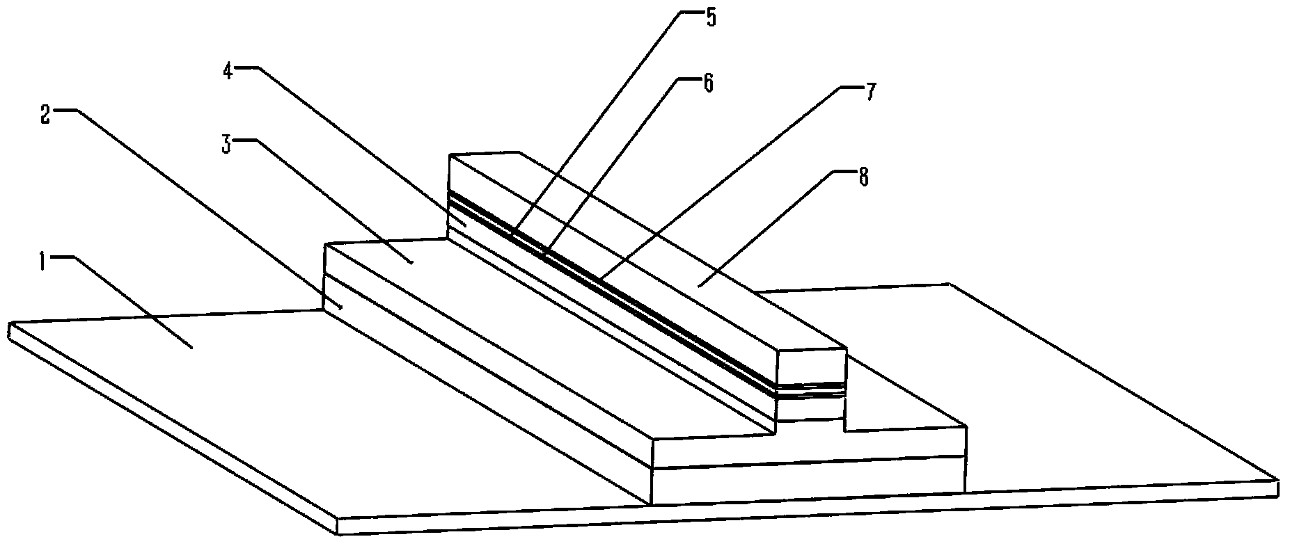
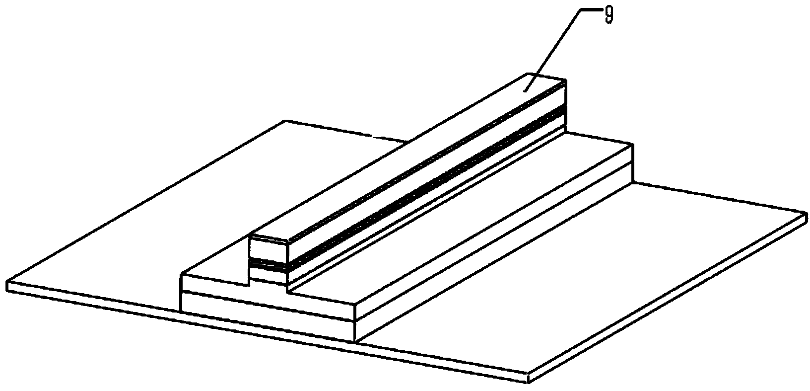
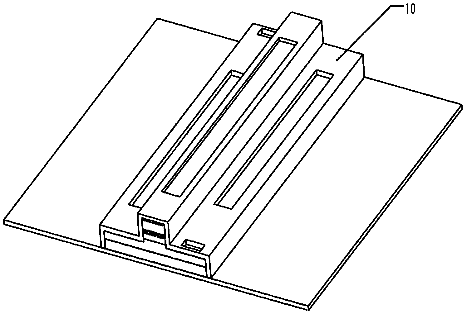
[0025] Said traveling wave electrode gradient coupled ridge waveguide InP double heterojunction phototransistor comprises: an InP substrate 1, an InP buffer layer 2, an InGaAsP sub-collector region 3, an InGaAsP collector region 4, an InGaAsP transition layer 5, an InGaAsP The base region 6, the InP emitter region 7, the InP cap layer 8, each layer is grown on the InP substrate 1 sequentially according to the sequence number from small to large; the InGaAs ohmic contact layer 9 is grown on the InP cap layer 8, and the polyimide Layer 10 includes the emitter and collector mesa of the device, opening the electrode window, an emitter 11, the first collector 12, the second collector 13, the third collector 14, and the fourth collector 15 by sputtering Manufactured on the InP substrate 1 and the polyimide layer 10, and then etched traveling wave electrodes;

[0026] T...


PUM


Abstract

The invention discloses a traveling wave electrode gradual change coupling ridge waveguide InP double-heterojunction photo transistor. A double-heterojunction structure is adopted, the traveling wave electrode gradual change coupling ridge waveguide InP double-heterojunction photo transistor comprises an (e-b) heterojunction which is composed of an InP emitter region and an InGaAsP base region and a (b-c) heterojunction which is composed of an InGaAsP base region and an InGaAsP collector region, and a traditional heterojunction photo transistor e-b junction single-heterojunction structure is replaced. The InGaAsP base region with high doping concentration is used as a photo-absorption layer of the double-heterojunction photo transistor. A gradual change coupling ridge waveguide structure which is formed by the InGaAsP base region, the InGaAsP collector region and an InGaAsP secondary collector region is adopted, so that probed light is detected and absorbed by a side edge, and the mode that traditional HPT light is in vertical incidence from the top end is replaced. The light transmission direction is perpendicular to the carrier transportation direction, and light absorption efficiency and working speed can be respectively optimized. A traveling wave electrode which is formed by an emitter electrode and a collector electrode is arranged, the distribution effect of a traditional electrode in the transmitting process of high-frequency signals can be effectively reduced, the influence of stray capacitance on high-speed transmission is decreased, and the working speed of the device is further increased.

Description

technical field [0001] The invention discloses an InP double heterojunction phototransistor (DHPT) with a traveling-wave electrode gradient coupling ridge waveguide, in particular to a traveling-wave electrode gradient coupling ridge waveguide phototransistor, which is a high-speed and high-responsive optoelectronic semiconductor device that can solve The contradiction between light absorption efficiency and operating speed of conventional heterojunction phototransistors (HPTs). Background technique [0002] In the microwave optical communication system, new applications such as high-speed detection and absorption of light, high-speed frequency mixing, signal locking and up-and-down conversion have higher and higher requirements on the optical receiver (Receiver). Satisfy the work of signal mixing and so on. In recent years, the rapid development of HPT detectors integrates the functions of light detection and electrical amplification, and has become a focus of research on ...

Claims


Application Information

Patent Timeline
Patent Type & Authority Applications(China)
IPC IPC(8): H01L31/11H01L31/0352H01L31/0304
CPCH01L31/03529H01L31/1105
Inventor 江之韵谢红云张良浩霍文娟张万荣
Owner BEIJING UNIV OF TECH
Why Eureka
Try Eureka