Fabrication method of monolithic integrated chip of laser array and combiner

A laser array, monolithic integration technology, applied in lasers, laser components, semiconductor lasers, etc., can solve the problems of reducing the yield of device manufacturing, increasing the complexity of device manufacturing, etc., to simplify the device manufacturing process and reduce optical diffraction loss. , the effect of reducing the size of the combiner

Active Publication Date: 2016-01-06
INST OF SEMICONDUCTORS - CHINESE ACAD OF SCI
View PDF6 Cites 3 Cited by
  • Summary
  • Abstract
  • Description
  • Claims
  • Application Information

AI Technical Summary

Problems solved by technology

This makes the etching of the two parts of the waveguide of the laser and the multiplexer need to be carried out step by step, which increases the complexity of device manufacturing and reduces the yield of device manufacturing.

Method used


Image

  • Fabrication method of monolithic integrated chip of laser array and combiner
  • Fabrication method of monolithic integrated chip of laser array and combiner
  • Fabrication method of monolithic integrated chip of laser array and combiner

Examples


Embodiment Construction

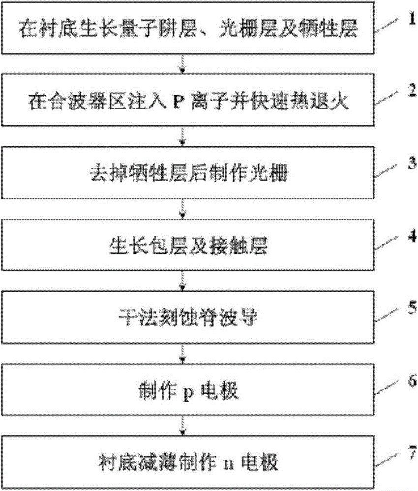
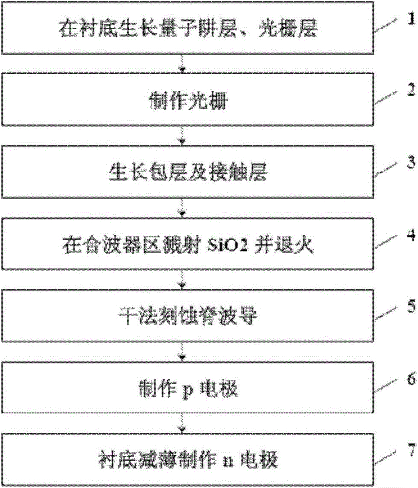
[0026] see figure 1 , is the first embodiment of the present invention, with reference to Figure 3 to Figure 8 As shown, the present invention provides a method for manufacturing a monolithic integrated chip of a laser array and a multiplexer, comprising the following steps:

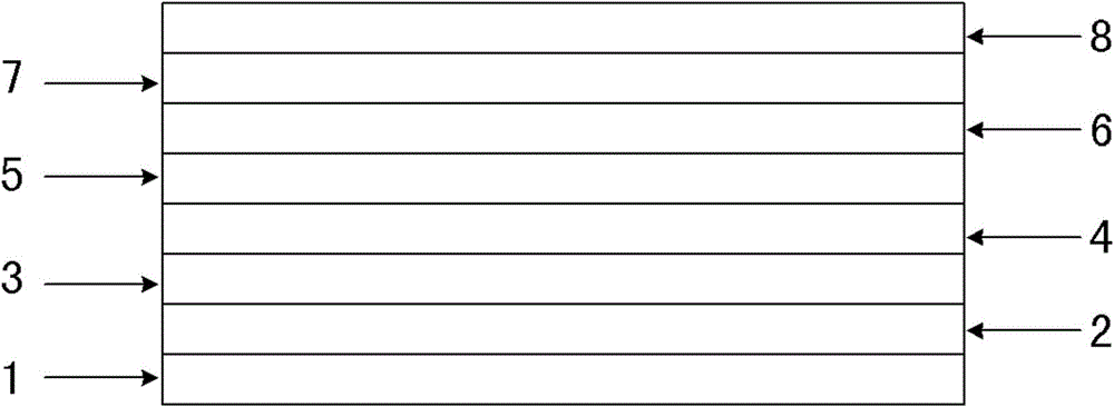
[0027] Step 1: On the n-type InP substrate 1, grow n-type InP buffer layer 2, n-type AlGaInAs cladding layer 3, AlGaInAs multi-quantum well layer 4, p-type AlGaInAs cladding layer 5, InP spacer layer 6, and InGaAsP grating layer 7 sequentially , InP sacrificial layer 8, forming the substrate, such as image 3 , one side of the substrate is the active region A, and the other side is the combiner region D, such as Figure 4 . The AlGaInAs multi-quantum well layer 4 includes more than two AlGaInAs quantum wells and two upper and lower AlGaInAs refractive index gradient layers. There may be no InP spacer layer 6 in the device;

[0028] Step 2: Implant P ions into the InP sacrificial layer 8 in the comb...


PUM


Abstract

A method for manufacturing a laser array and combiner monolithic integration chip comprises the steps that an n-type InP buffer layer, an n-type AlGaInAs covering layer, an AlGaInAs multi-quantum well layer, a p-type AlGaInAs covering layer, an InP interlayer, an InGaAsP grating layer and an InP sacrificial layer are grown on an n-type InP substrate in sequence to form a substrate, an active region is arranged on one side of the base chip, and a combiner region is arranged on the other side of the substrate; P ions are injected into the InP sacrificial layer of the combiner region, and fast thermal annealing is carried out; the InP sacrificial layer is removed, and gratings are manufactured in the InGaAsP grating layer of the active region; a p-type InP covering layer and a p-type InGaAs contact layer are grown on the InGaAsP grating layer of the active region and the InGaAsP grating layer of the combiner region; the p-type InGaAs contact layer, the p-type InP covering layer, the InGaAsP grating layer and the InP interlayer are removed through dry etching, ridge type waveguides of all laser units are formed in the active region, and combiner ridge type waveguides are formed in the combiner region; p electrodes are manufactured on the ridge type waveguides of the active region; the n-type InP substrate is thinned, an n electrode is manufactured on the back face of the n-type InP substrate, and manufacturing is completed.

Description

technical field [0001] The invention relates to the field of optoelectronic devices, in particular to a method for manufacturing a monolithic integrated chip of a laser array and a multiplexer. Background technique [0002] The multi-wavelength laser with monolithic integrated passive optical multiplexer is the core device of modern wavelength division multiplexing (WDM) optical communication system, which has the advantages of compact structure, low optical and electrical connection loss, high stability and reliability. This monolithic integrated device includes two parts: a laser array and a multiplexer. The light emitted by each laser is combined by the multiplexer and output by a single waveguide. The fabrication of the laser array requires that each laser has a different emission wavelength, and the fabrication of the multiplexer requires that the light can be transmitted in it with low loss. Therefore, the emission wavelength of the material of the multiplexer is gener...

Claims


Application Information

Patent Timeline
Patent Type & Authority Patents(China)
IPC IPC(8): H01S5/343H01S5/22
Inventor 梁松朱洪亮王圩
Owner INST OF SEMICONDUCTORS - CHINESE ACAD OF SCI
Why Eureka
Try Eureka