

Wafer level packaging method for micro electromechanical system (MEMS) chip and single-chip micro-miniature type MEMS chip
A wafer-level packaging, ultra-small technology, applied in the field of single-chip ultra-small MEMS chips, can solve the problems of large chip area, high cost, low efficiency, etc., and achieve the effect of reducing area, low cost and simple process flow
- Summary
- Abstract
- Description
- Claims
- Application Information
AI Technical Summary
Problems solved by technology
Method used
Image

Examples
Embodiment 1
[0041] (1) Formation of TSV wafers:
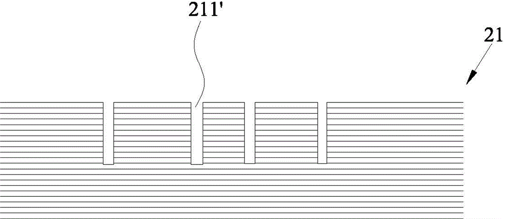
[0042] The material of the first wafer 21 is heavily doped single crystal silicon with a resistivity of about 0.01 Ω·cm, which is a good conductive material. Such as figure 2 As shown, grooves 211' are formed on the first wafer 21 through semiconductor processing processes such as glue coating, exposure, development, etching, and glue removal. The depth of the grooves 211' is 50 μm, and the cross-sectional pattern of the grooves 211' is circular ;
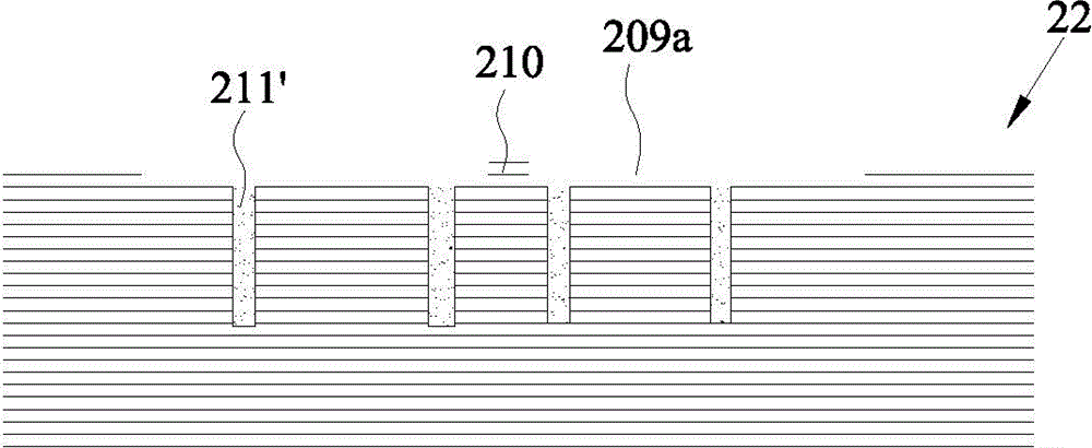
[0043] The insulating material silicon dioxide is filled in the groove 211' by chemical vapor deposition, and then the insulating material outside the groove 211' is removed by reverse etching, so that only the insulating material is arranged in the groove 211', such as image 3 As shown; then, the upper cavity 209a is etched by common semiconductor processing technology, and the depth of the upper cavity 209a is 1 μm; when the upper cavity 209a is etched, a part is left unetched in the mid...
Embodiment 2
[0061] (1) Formation of TSV wafers:
[0062] The material of the first wafer 21 is heavily doped single crystal silicon with a resistivity of about 0.01 Ω·cm, which is a good conductive material. Such as figure 2 As shown, grooves 211' are formed on the first wafer 21 through semiconductor processing processes such as glue coating, exposure, development, etching, and glue removal. ;
[0063] Deposit the insulating material silicon dioxide in the groove 211' by filling the glass paste, then remove the insulating material outside the groove 211', heat and sinter, so that only the insulating material is in the groove 211', such as image 3 As shown; then, the upper cavity 209a is etched by common semiconductor processing technology, and the depth of the upper cavity 209a is 5 μm; when the upper cavity 209a is etched, a part is left unetched in the middle to form a bond The blocks 210 are combined to form a TSV wafer 22 .
[0064] (2) Formation of the first bonded wafer: ...
PUM
| Property | Measurement | Unit |
|---|---|---|
| depth | aaaaa | aaaaa |
| depth | aaaaa | aaaaa |
| electrical resistivity | aaaaa | aaaaa |
Abstract
Description
Claims
Application Information