Tunneling field effect transistor and preparation method thereof

A tunneling field effect, transistor technology, applied in semiconductor/solid-state device manufacturing, diodes, semiconductor devices, etc., can solve problems such as low bipolar effect of driving current, suppress bipolar effect, increase driving current, The effect of reducing the subthreshold current

Active Publication Date: 2014-02-05
SHANGHAI INST OF MICROSYSTEM & INFORMATION TECH CHINESE ACAD OF SCI
View PDF3 Cites 11 Cited by
  • Summary
  • Abstract
  • Description
  • Claims
  • Application Information

AI Technical Summary

Problems solved by technology

[0004] In view of the shortcomings of the prior art described above, the purpose of the present invention is to provide a tunneling field effect transistor and its preparation method, which are used to solve the problem of low driving current and bipolar effect of ordinary tunneling field effect transistors in the prior art. The problem

Method used


Image

  • Tunneling field effect transistor and preparation method thereof
  • Tunneling field effect transistor and preparation method thereof
  • Tunneling field effect transistor and preparation method thereof

Examples


Embodiment 1

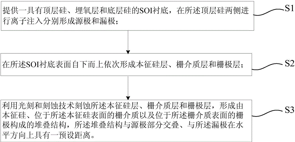
[0044] The invention provides a method for preparing a tunneling field effect transistor, such as figure 1 As shown in the flowchart of the preparation method, the preparation method of the tunneling field effect transistor at least includes the following steps:

[0045] S1, providing an SOI substrate with a top layer of silicon, a buried oxide layer and a bottom layer of silicon, performing ion implantation on both sides of the top layer of silicon to form a source and a drain respectively;

[0046] S2, sequentially forming an intrinsic silicon layer, a gate dielectric layer and a gate layer on the surface of the SOI substrate from bottom to top;

[0047] S3, using photolithography and etching techniques to etch the intrinsic silicon layer, gate dielectric layer, and gate layer to form intrinsic silicon, a gate dielectric on the surface of the intrinsic silicon, and a gate electrode on the surface of the gate dielectric. A stacked structure composed of electrodes, the stacke...

Embodiment 2

[0068] The present invention also provides a tunneling field effect transistor, which is made by using the preparation method provided in Embodiment 1, and the tunneling field effect transistor at least includes:

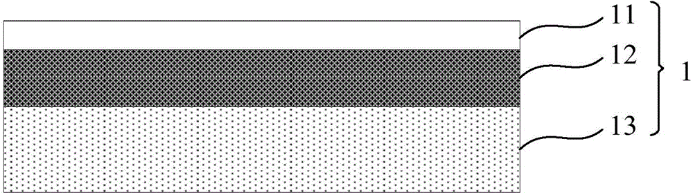
[0069] SOI substrate 1, said SOI substrate 1 comprises top layer silicon 11, buried oxide layer 12 and bottom layer silicon 13;

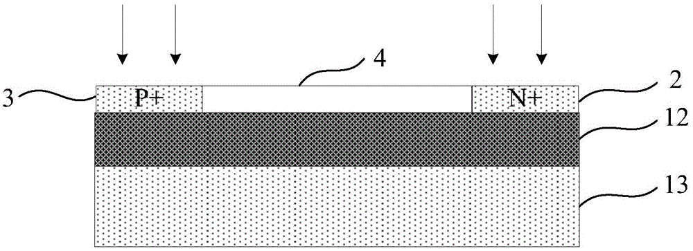
[0070] The source 3 and the drain 2 are respectively formed on both sides of the top layer silicon 11;

[0071] A stacked structure, formed on the SOI substrate 1, the stacked structure includes intrinsic silicon 8, a gate dielectric 9 located on the surface of the intrinsic silicon 8, and a gate 10 located on the surface of the gate dielectric 9; The stacked structure partially overlaps the source 3 and has a predetermined distance from the drain 2 in the horizontal direction.

[0072] The stacked structure formed is as Figure 5 As shown, the stacked structure partially overlaps with the source 3 and has a predetermined distance from ...


PUM


Abstract

The invention provides a tunneling field effect transistor and a preparation method thereof. The preparation method at least comprises the following steps that an SOI substrate provided with top layer silicon, an oxygen buried layer and bottom layer silicon is provided, and ion injection is conducted on the two sides of the top layer silicon to form a source electrode and a drain electrode respectively; an intrinsic silicon layer, and a grid medium layer and a grid layer are sequentially formed on the surface of the SOI substrate from bottom to top; a stacking structure is formed by etching the intrinsic silicon layer, the grid medium layer and the grid layer through the photoetching and etching technologies, the stacking structure is partially overlapped with the source electrode and is preset distance away from the drain electrode in the horizontal direction. According to the tunneling field effect transistor and the preparation method of the tunneling field effect transistor, the stacking structure is overlapped with the source electrode so that the tunneling area can be increased, and further a driving current is increased. In addition, the stacking structure is preset distance away from the drain electrode in the horizontal direction, and the bipolar effect in the tunneling field effect transistor can be suppressed through the preset distance, and a subthreshold current is reduced.

Description

technical field [0001] The invention relates to the technical field of semiconductor devices, in particular to a tunneling field effect transistor and a preparation method thereof. Background technique [0002] In recent years, microelectronics technology with silicon integrated circuits as the core has developed rapidly. The development of integrated circuit chips basically follows Moore's law, that is, the integration level of semiconductor chips doubles every 18 months. Over the past period of time, the advancement of microelectronics technology has been based on the continuous optimization of the cost-effectiveness of materials, processes and processes. However, scaling down conventional silicon-based CMOS transistors has become increasingly difficult with the development of microelectronics technology. Moreover, most electronic products manufactured using MOSFETs today have the following main problems: First, due to the shortening of the MOSFET channel, the leakage cur...

Claims


Application Information

Patent Timeline
Patent Type & Authority Applications(China)
IPC IPC(8): H01L29/78H01L21/336H01L29/06
CPCH01L29/423H01L29/66356H01L29/7391
Inventor 刘畅俞文杰赵清太王曦
Owner SHANGHAI INST OF MICROSYSTEM & INFORMATION TECH CHINESE ACAD OF SCI
Why Eureka
Try Eureka