Method for packaging cadmium zinc telluride pixel detector module

A packaging method, cadmium zinc telluride technology, applied in the direction of semiconductor devices, semiconductor/solid-state device manufacturing, electrical components, etc., can solve the problems of pixel electrode mechanical damage, large glue spots, poor bonding force of solder joints, etc., to reduce the external environment And the influence of external force, the effect of overcoming the open circuit problem and overcoming the short circuit problem

Active Publication Date: 2014-02-05
IMDETEK
View PDF3 Cites 6 Cited by
  • Summary
  • Abstract
  • Description
  • Claims
  • Application Information

AI Technical Summary

Problems solved by technology

[0003] The traditional wire welding connection technology is not suitable for the packaging connection of CdZnTe pixel detector modules with more pixels due to the limitation of the operating space, and the bonding force of the solder joints of this method is poor
However, in the method of manufacturing CdZnTe pixel detector module by metal flip-chip welding technology, the temperature during welding needs to be above 140 degrees, which affects the physical properties of the chip, and at the same time, it is easy to cause mechanical damage to the pixel electrode during welding.
The document "V.Jordanov, J.Macri, J.Clayton, et al. Nuclear Instruments and Methods in Physics Research A, 2001, 458:511-517." discloses a CdZnTe pixel detector prepared by screen printing technology The method of the sensor module, the method adopts the polymer conductive adhesive connection technology, that is, the corresponding surface of the pixel electrode surface of the CdZnTe pixel detector element and the ceramic or printed circuit board (Printed Circuit Board, referred to as PCB) substrate are printed by screen printing. Silver conductive glue of corresponding size is printed on the electrode, and then the two are fixed by one-to-one flip-chip connection technology. The temperature during preparation is 80 degrees. Control the relative position between the glue dots, so that the flip-mounted CdZnTe pixel detector module is prone to short circuit or open circuit of the pixel electrode

Method used


Image

  • Method for packaging cadmium zinc telluride pixel detector module
  • Method for packaging cadmium zinc telluride pixel detector module
  • Method for packaging cadmium zinc telluride pixel detector module

Examples


Embodiment 1

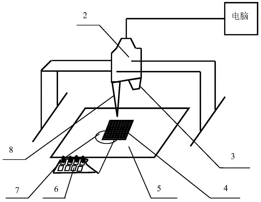
[0020] Step 1, using a CdZnTe single wafer to prepare an 8×8 array of CdZnTe pixel detector elements 1 . The substrate 4 for flip-chip connection corresponding to the size of the pixel electrode is designed. Then fix the substrate 4 made of PCB on the base 5 of the three-dimensional automatic dispensing machine, observe the position information of the substrate 4 through the CCD3 and transmit it to the computer, select the 8×8 matrix dispensing mode, and select the X-axis step to 1mm, The step of the Y axis is 1 mm, and input to the computer, the computer completes the matrix dispensing by controlling the movement of the three-dimensional translation platform 2, uniformly coats the silver conductive glue 7 on the metal electrode 6 of the substrate 4, and controls the single flow through the flow controller 8 The amount of dispensing.

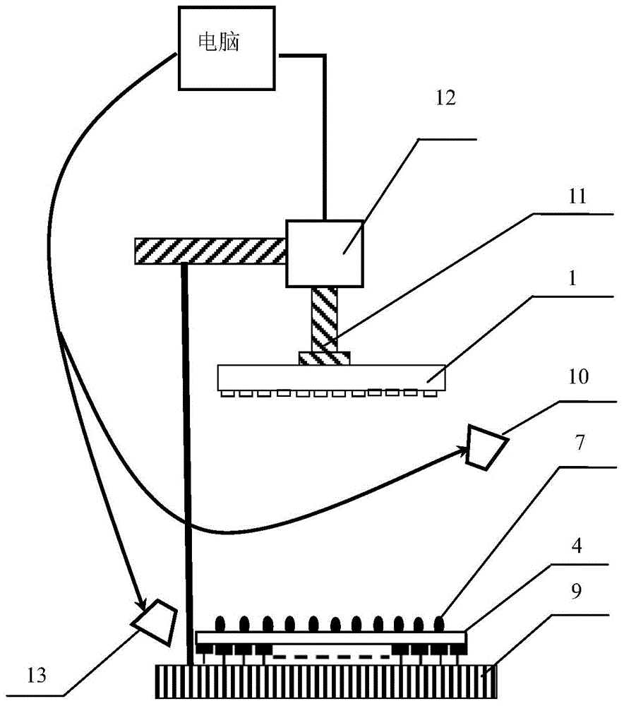
[0021] Step 2: Place the glued substrate 4 on the reference table 9 of the flip-chip bonding apparatus, record the image information on the su...

Embodiment 2

[0027] Step 1, using a CdZnTe single wafer to prepare a 20×20 array of CdZnTe pixel detector elements 1 . The substrate 4 for flip-chip connection corresponding to the size of the pixel electrode is designed. Then fix the ceramic substrate 4 on the base 5 of the three-dimensional automatic dispensing machine, observe the position information of the substrate 4 through the CCD3 and transmit it to the computer, select the 20×20 matrix dispensing mode, and select the X-axis step to 350 μm, The Y-axis step is 350 μm, and the step parameters are input into the computer. The computer completes the matrix dispensing by controlling the movement of the three-dimensional translation platform 2, and uniformly coats the silver conductive glue 7 on the metal electrode 6 of the substrate 4, and passes through the flow controller. 8 Control the amount of single dispensing.

[0028] Step 2: Place the glued substrate 4 on the reference table 9 of the flip-chip bonding apparatus, record the im...


PUM


Abstract

The invention discloses a method for packaging a cadmium zinc telluride pixel detector module. The method is used for solving the technical problem that according to an existing method for packaging the cadmium zinc telluride pixel detector module, the relative position accuracy of connecting adhesive points is poor. According to the technical scheme, a silver conductive adhesive is adopted as an inversion connecting medium, a three-dimensional automatic adhesive dispenser is utilized for accurately controlling the size and the relative position of the adhesive points in a matrix adhesive dispensing mode, an inversion welding instrument is also utilized for controlling accurate walking of a transmission system in a two-CCD framing and focusing working mode, the problem that pixel electrodes on a cadmium zinc telluride pixel electrode detector element are correspondingly connected with metal electrodes on a substrate in a one-to-one mode is solved, and the short-circuit or breaking phenomenon of the pixel electrodes is avoided. Due to the adoption of the program-controlled matrix adhesive dispensing mode, the relative position between the adhesive points is effectively controlled, the precision reaches 10 micrometers, meanwhile, due to the adoption of a flow controller, the size of the obtained minimum adhesive point is 150 micrometers, and the short-circuit problem of the pixel electrodes is effectively solved.

Description

technical field [0001] The invention relates to a method for packaging a module, in particular to a method for packaging a CdZnTe pixel detector module. Background technique [0002] CdZnTe crystal, as a ternary solid solution compound semiconductor with excellent photoelectric properties, has become the most ideal material for the preparation of room temperature nuclear radiation detectors, and can be widely used in nuclear medicine diagnosis, environmental monitoring, industrial nondestructive testing, safety inspection, nuclear weapon breakthrough, etc. defense, astrophysics, and high-energy physics. However, connecting the CdZnTe crystal with the pixel electrodes to the substrate to form a detector module is the key to realize the application in the field of X-ray and γ-ray imaging. [0003] The traditional wire welding connection technology is not suitable for the packaging connection of CdZnTe pixel detector modules with more pixels due to the limitation of the operat...

Claims


Application Information

Patent Timeline
Patent Type & Authority Applications(China)
IPC IPC(8): H01L31/18H01L31/0203H01L31/09
CPCH01L21/681H01L31/1832
Inventor 徐亚东何亦辉齐阳谷亚旭王涛查钢强介万奇
Owner IMDETEK
Why Eureka
Try Eureka