Positioning tool for chip welding

A technology for positioning tooling and chip welding, applied in welding equipment, auxiliary welding equipment, welding/cutting auxiliary equipment, etc., can solve the problems of chip position offset, high chip welding void rate, etc., achieve firm welding, improve quality and performance, Effect of reducing void ratio

Inactive Publication Date: 2014-02-12
XIAN YONGDIAN ELECTRIC
View PDF6 Cites 10 Cited by
  • Summary
  • Abstract
  • Description
  • Claims
  • Application Information

AI Technical Summary

Problems solved by technology

[0004] The invention provides a positioning tool for chip welding, which solves the technical problems in the prior art that position deviation is easy to occur during chip welding and the void rate of chip welding is high

Method used


Image

  • Positioning tool for chip welding
  • Positioning tool for chip welding
  • Positioning tool for chip welding

Examples


Embodiment Construction

[0011] The present invention will be further described in detail below through specific embodiments and in conjunction with the accompanying drawings.

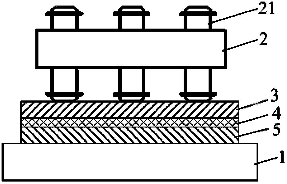
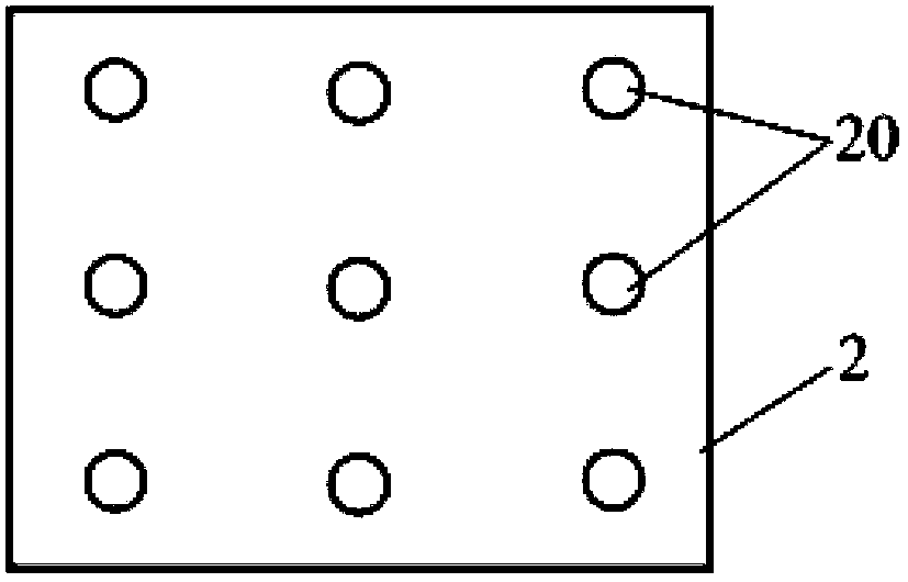
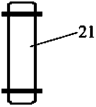
[0012] figure 1 It is a schematic diagram of the overall structure of a positioning tool for chip bonding according to an embodiment of the present invention. figure 2 It is a top view of the top cover in the positioning tool for chip bonding according to the embodiment of the present invention. image 3 It is a front view of a positioning pin in a positioning tool for chip bonding according to an embodiment of the present invention. Such as Figure 1 to Figure 3 As shown in , a positioning tool for chip bonding provided by an embodiment of the present invention includes a base 1 and a top cover 2 located above the base 1, wherein the top cover 2 is provided with several positioning holes 20, each The positioning hole 20 is provided with a positioning pin 21 that can freely slide up and down in the positioning hole, and on...


PUM


Abstract

The invention discloses a positioning tool for chip welding. The positioning tool comprises a base and a top cover positioned above the base, wherein a plurality of positioning holes are formed in the top cover, a positioning pin capable of sliding in each of the positioning holes vertically is arranged in each of the positioning holes, and one end of the positioning pin close to the base is used for abutting against chips to be welded. By arranging a plurality of positioning pins formed in the top cover and sliding freely to apply a certain pressure on the chips to be welded, the chips, welding lugs and a DBC base plate are fixed relatively, and the chips cannot be damaged by pressing. Therefore, position offset of the chips during welding is avoided, voidage of chip welding is reduced, the welding is firm, and quality and performance of welded products are effectively improved.

Description

technical field [0001] The invention relates to semiconductor packaging technology, in particular to a positioning tool for chip welding. Background technique [0002] Today, semiconductor packaging technology is continuously developing in the direction of high density, high speed, and high reliability. Insulated Gate Bipolar Transistor (full English name: Insulated Gate Bipolar Transistor, referred to as IGBT) is a composite fully-controlled voltage-driven power semiconductor device composed of a bipolar transistor (BJT) and an insulated gate field effect transistor (MOS). , Insulated gate bipolar transistors are internationally recognized as the most representative products of the third revolution of power electronics technology because of their high frequency, high voltage, high current, and easy on and off characteristics. The packaging process of insulated gate bipolar transistors involves several key technologies, among which the welding of the chip and the thermally ...

Claims


Application Information

Patent Timeline
Patent Type & Authority Applications(China)
IPC IPC(8): B23K37/04H01L21/68
CPCB23K37/0408B23K2101/40H01L21/68
Inventor 梁杰
Owner XIAN YONGDIAN ELECTRIC
Why Eureka
Try Eureka