Thin film super absorber with low cost and large area and preparation method of film

A large-area thin-film, super-absorbing technology, applied in metal material coating process, superimposed layer plating, layered products, etc., can solve problems such as being unsuitable for super-large area preparation, and achieve a simple, easy-to-implement method and broad commercial prospects. , the effect of low cost

Inactive Publication Date: 2014-02-12
FUDAN UNIV
View PDF4 Cites 14 Cited by
  • Summary
  • Abstract
  • Description
  • Claims
  • Application Information

AI Technical Summary

Problems solved by technology

But both techniques still have their limitations
For example, anodized aluminum oxide films and spin-coating operations are still not suitable for the needs o

Method used


Image

  • Thin film super absorber with low cost and large area and preparation method of film
  • Thin film super absorber with low cost and large area and preparation method of film
  • Thin film super absorber with low cost and large area and preparation method of film

Examples


Embodiment 1

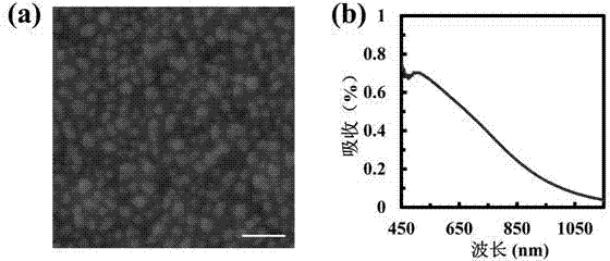
[0031] Example 1: Glass substrate / silver mirror / SiO 2 Dielectric layer / regular nanoparticles

[0032] (1) With the glass substrate as the substrate, a 100 nm thick flat Ag film is plated in the magnetron sputtering equipment, and 90 nm SiO is sputtered on it 2 membrane.

[0033] (2) In Ag / SiO 2 Continue to sputter a silver film with a nominal thickness of 6 nm on the film. Since the thickness is much smaller than the permeation threshold, the actual film layer does not form a continuous flat film, but random regular-shaped silver nano-islands.

[0034] (3) figure 2 (b) is the measured optical absorption spectrum, and the results show that the absorption peak of the absorber reaches more than 70%, and the absorption has a broad-spectrum property in the visible light band.

Embodiment 2

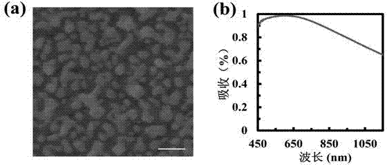
[0035] Example 2: Glass substrate / silver mirror / SiO 2 Dielectric layer / irregular nanoparticles

[0036] (1) With the glass substrate as the substrate, a 100 nm thick flat Ag film is plated in the magnetron sputtering equipment, and 90 nm SiO is sputtered on it 2 membrane.

[0037] (2) In Ag / SiO 2 Continue to sputter a silver film with a nominal thickness of 9 nm on the film. Since the thickness is slightly smaller than the permeation threshold, the actual film layer does not form a continuous flat film, but forms metal nanoparticles, and the air gap between the particles is much smaller than figure 2 structure shown in .

[0038] (3) image 3 (b) is the measured optical absorption spectrum. The results show that the three-layer structure achieves 100% optical absorption, and the ultrahigh absorption has ultra-broadband characteristics in the visible and near-infrared bands.

Embodiment 3

[0039] Embodiment 3: glass substrate / silver mirror / SiO 2 Dielectric layer / silver nanomesh

[0040] (1) With the glass substrate as the substrate, a 100 nm thick flat Ag film is plated in the magnetron sputtering equipment, and 90 nm SiO is continuously sputtered on it 2 membrane.

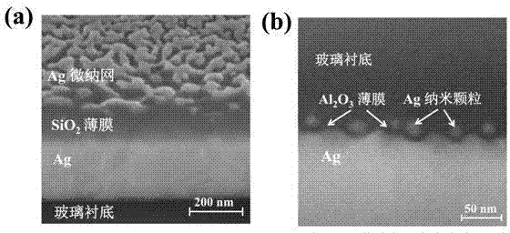
[0041] (2) In Ag / SiO 2 Continue to sputter a silver film with a nominal thickness of 12 nm on the film. Since the thickness is greater than the permeation threshold, although the actual film layer does not form a continuous flat film, the surface morphology formed is no longer discrete silver nano-islands, but interconnected. connected silver nanomesh, such as figure 1 (a) shown. The network structure combined with the underlying continuous metal film can be conveniently used as two electrodes of a photoelectric device.

[0042] (3) Figure 4 (a) is a photo taken of the sample under white light irradiation. The photo shows darker colors, while only faint blue light is reflected by the ...


PUM

PropertyMeasurementUnit
Thicknessaaaaaaaaaa
Diameteraaaaaaaaaa
Thicknessaaaaaaaaaa

Abstract

The invention belongs to the technical field of micro-nano photons, and particularly relates to a thin film super absorber with the low cost and a large area and a preparation method of the film. The method is based on widely used film coating and thermal annealing methods, a metal particle array or a micro-nano net structure with a controllable integral shape is prepared as a coupling micro-nano antenna of a three-layer or five-layer thin-film type artificial specific material super absorber, and the thin film super absorber is a super absorbing thin film capable of realizing operation from the visible light band to the infrared band. According to the method, an expensive and complicated electronic etching technology is eliminated, and the preparation with the large area and the low cost can be carried out. The technology is simple in operation, and can be compatible with various substrates, and has a wide commercial prospect in the fields of solar energy collection, heat energy circulation, photochemical catalyst reinforcement, thin-film photoelectronic devices.

Description

technical field [0001] The invention belongs to the field of micro-nano photon technology, and in particular relates to a low-cost large-area thin-film superabsorber and a preparation method thereof. Background technique [0002] High-efficiency, band-tunable electromagnetic wave absorbing materials are very important for radar protection, photon collection, thermal energy cycle, vacuum heat dissipation and other fields. How to realize lightweight and large-area thin-film absorbent materials is a research hotspot today. In recent years, optical metamaterials have made great progress in thin-film superabsorbers, but most artificial meta-film materials are based on costly micro-nano electron beam etching technology. However, due to the limitations of these fabrication techniques, metamaterial superabsorbers are difficult to fabricate in large areas and develop corresponding practical applications. In 2012, literature reported that two technologies broke this bottleneck. The...

Claims


Application Information

Patent Timeline
IPC IPC(8): B32B33/00C23C28/00
Inventor 甘巧强江素华刘恺
Owner FUDAN UNIV
Why Eureka
Try Eureka