
Copper plating solution for PCB (printed circuit board) through holes, and preparation method and plating method thereof

A through-hole electroplating and copper solution technology, which is applied in the direction of electrical connection formation of printed components, can solve the problems of poor plating ability of copper plating layer, uneven copper plating layer, poor ductility, gloss and toughness, etc.

Inactive Publication Date: 2014-02-12
东莞市富默克化工有限公司
View PDF2 Cites 28 Cited by
  • Summary
  • Abstract
  • Description
  • Claims
  • Application Information

AI Technical Summary

Problems solved by technology

[0005] When the electroplating liquid in the prior art electroplates PCB through-holes, the copper-plated layer obtained has poor plating ability, and the copper-plated layer is uneven, and ductility, gloss and toughness are relatively poor. Therefore, it is necessary to develop a A PCB through-hole electroplating copper solution with good uniform plating ability, flat copper layer, good ductility, gloss and toughness, and preparation method and use method thereof

Method used


Image

  • Copper plating solution for PCB (printed circuit board) through holes, and preparation method and plating method thereof
  • Copper plating solution for PCB (printed circuit board) through holes, and preparation method and plating method thereof
  • Copper plating solution for PCB (printed circuit board) through holes, and preparation method and plating method thereof

Examples


Embodiment 1

[0082] A copper electroplating solution for PCB through holes, each component of the copper electroplating solution and its content are:

[0083] Copper sulfate pentahydrate: 70g / L

[0084] Sulfuric acid: 105g / L

[0085] Chloride ion: 30ppm

[0086] Brightener: 5g / L

[0087] Carrier: 3g / L

[0088] Leveling agent: 2g / L

[0089] Deionized water balance;

[0090] And the concentration ratio of copper sulfate pentahydrate to sulfuric acid is 1:1.5.

[0091] The brightener is a mixture of 2-mercaptobenzimidazole and ethylenethiourea with a weight ratio of 1.5:1; the carrier is polyethylene glycol with a molecular weight of 2000.

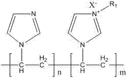
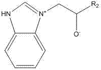
[0092] The leveling agent is a mixture of leveling agent A and leveling agent B with a weight ratio of 1.2:1; wherein, the leveling agent A is a polyvinylimidazolium quaternary ammonium compound, and the leveling agent B is N- Polymer of vinylimidazole and epoxy compound.

[0093] The structural formula of the leveling agent A is:

[0094]

[...

Embodiment 2

[0108] A copper electroplating solution for PCB through holes, each component of the copper electroplating solution and its content are:

[0109] Copper sulfate pentahydrate: 90g / L

[0110] Sulfuric acid: 150g / L

[0111] Chloride ion: 45ppm

[0112] Brightener: 15g / L

[0113] Carrier: 10g / L

[0114] Leveling agent: 5g / L

[0115] Deionized water balance;

[0116] And the concentration ratio of copper sulfate pentahydrate to sulfuric acid is 1:1.67.

[0117] The brightener is a mixture of 2-mercaptobenzimidazole and ethylenethiourea in a weight ratio of 2:1; the carrier is polyethylene glycol with a molecular weight of 3500.

[0118] The leveling agent is a mixture of leveling agent A and leveling agent B with a weight ratio of 1.5:1; wherein, the leveling agent A is a polyvinylimidazolium quaternary ammonium compound, and the leveling agent B is N- Polymer of vinylimidazole and epoxy compound.

[0119] The structural formula of the leveling agent A is:

[0120]

[0...

Embodiment 3

[0134] A copper electroplating solution for PCB through holes, each component of the copper electroplating solution and its content are:

[0135] Copper sulfate pentahydrate: 110g / L

[0136] Sulfuric acid: 200g / L

[0137] Chloride ion: 60ppm

[0138] Brightener: 25g / L

[0139] Carrier: 15g / L

[0140] Leveling agent: 10g / L

[0141] Deionized water balance;

[0142] And the concentration ratio of copper sulfate pentahydrate to sulfuric acid is 1:1.82.

[0143] The brightener is a mixture of 2-mercaptobenzimidazole and ethylenethiourea with a weight ratio of 2.5:1; the carrier is polyethylene glycol with a molecular weight of 5000.

[0144] The leveling agent is a mixture of leveling agent A and leveling agent B with a weight ratio of 1.8:1; wherein, the leveling agent A is a polyvinylimidazolium quaternary ammonium compound, and the leveling agent B is N- Polymer of vinylimidazole and epoxy compound.

[0145] The structural formula of the leveling agent A is:

[0146] ...


PUM

PropertyMeasurementUnit
melting pointaaaaaaaaaa

Abstract

The invention relates to the technical field of PCB (printed circuit board) plating, in particular to a copper plating solution for PCB through holes, and a preparation method and a plating method thereof. Each liter of the copper plating solution comprises the following components according to contents: 70-150g of copper sulfate pentahydrate, 100-300g of sulfuric acid, 30-100ppm of chlorine ions, 5-50g of brightener, 3-30g of carrier, 2-20g of leveling agent and the balance of deionized water, wherein the concentration ratio of the copper sulfate pentahydrate to the sulfuric acid is 1: (1.5-2). The plating method comprises the following steps: putting a PCB with through holes into a plating bath with the copper plating solution; plating during air agitation to obtain a copper plating layer. The copper plating layer formed by the plating method has a good uniform plating capability as high as 95% above, and is dense, smooth, relatively good in malleability, good in gloss, high in toughness and low in internal stress.

Description

technical field [0001] The invention relates to the technical field of PCB electroplating, in particular to a PCB through-hole copper electroplating solution, a preparation method thereof, and an electroplating method. Background technique [0002] The acidic sulfate copper plating process is widely used in the metallization of printed board holes because of its simple basic composition, stable solution, high current efficiency, and the addition of appropriate additives to obtain a bright, smooth, and tough copper plating layer. [0003] my country is now the world's largest producer of PCB boards, but my country's PCB board production is still at the low end of the industry. Domestically produced PCB boards are mainly low-end PCB boards, and high-end PCB boards are produced no matter from equipment or Raw materials are controlled by people. Foreign dye-based additives are generally relatively expensive, and the cost is high for the production of low-end PCB boards. Therefo...

Claims


Application Information

Patent Timeline
Patent Type & Authority Applications(China)
IPC IPC(8): C25D3/38C25D5/56H05K3/42
Inventor 王维仁伊洪坤
Owner 东莞市富默克化工有限公司
Learn More