Light emitting diode flip chip packaging method based on through hole technology

A light-emitting diode and chip packaging technology, applied in electrical components, circuits, semiconductor devices, etc., can solve the problems of poor contact, falling off, and thermal expansion and fracture of gold wire solder joints, and achieve compact structure, improved reliability, and size structure. compact effect

Active Publication Date: 2014-02-12
SHANGHAI UNIV
View PDF4 Cites 13 Cited by
  • Summary
  • Abstract
  • Description
  • Claims
  • Application Information

AI Technical Summary

Problems solved by technology

At present, most of the LED failures are not caused by the failure of the LED chip itself, but by poor contact, shedding, thermal expansion and fracture of the packaged gold wire solder joints, etc.

Method used


Image

  • Light emitting diode flip chip packaging method based on through hole technology
  • Light emitting diode flip chip packaging method based on through hole technology
  • Light emitting diode flip chip packaging method based on through hole technology

Examples


Embodiment 1

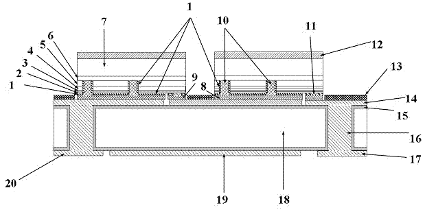
[0030] see figure 1 , figure 2 , image 3 , a flip-chip light-emitting diode chip packaging method based on through-hole technology, the process steps are as follows:

[0031] 1) On the sapphire substrate 7, n-type GaN6, light-emitting layer 5, p-type GaN4, ITO current spreading layer 3, and reflective layer 2 are sequentially grown to complete the fabrication of the light-emitting diode chip;

[0032] 2) Make blind holes on the light-emitting diode chip by etching technology or laser technology, and make through holes on the silicon substrate 18; then make the chip insulating layer 1 on the surrounding walls of the blind holes of the chip by physical chemical vapor deposition, Fabricate the substrate insulating layer 15 on the through hole peripheral wall of the silicon substrate 18, etch the chip insulating layer 1 on the bottom surface of the blind hole of the chip by plasma etching to expose the n-type GaN 6 , and then place it on the blind hole of the chip by evaporati...

Embodiment 2

[0048] This embodiment is basically the same as Embodiment 1, the difference is that the silicon substrate 18 is replaced with a ceramic base substrate, such as an alumina substrate, an AlN substrate, and in Embodiment 1, the substrate insulating layer 15 before the metallization of the silicon substrate 18 is made The process is no longer needed, and everything else is the same.


PUM


Abstract

The invention relates to a light emitting diode flip chip packaging method based on a through hole technology and a manufacturing process thereof. A light emitting diode comprises an LED flip chip, a substrate and a fluorescent glue layer. A light emitting diode flip chip packaging technology and the manufacturing process of the LED flip chip are provided to overcome the heat dissipation defect of an existing high-power LED. By means of an etching technology or a laser technology, the LED flip chip and the silicon substrate are respectively provided with a blind hole electrode and a through hole bonding pad, and the light emitting diode flip chip and the through hole substrate are obtained. By means of the shape design of a soldering-resistant layer, self alignment of the flip chip and the through hole substrate is convenient to achieve. Besides, the method does not need gold bonding, is simple in process and low in cost, improves heat dissipation performance by means of through holes, and improves reliability of LED chip packaging.

Description

technical field [0001] The invention relates to a flip-chip LED chip packaging method based on through-hole technology, and belongs to the technical field of chip packaging. Background technique [0002] As a new generation of lighting source, LED has three advantages of high luminous efficiency, long life, and environmental protection. With the continuous improvement of epitaxy and packaging technology, LED has been gradually applied in the field of general lighting. At present, most of the LED failures are not caused by the failure of the LED chip itself, but by poor contact, shedding, thermal expansion and fracture of the packaged gold wire solder joints. With the development of high-integration packaging trends, the requirements for reliability are getting higher and higher. Therefore, how to improve the reliability of LED packaging devices is a very difficult but must be solved bottleneck. Contents of the invention [0003] The object of the present invention is to p...

Claims


Application Information

Patent Timeline
Patent Type & Authority Applications(China)
IPC IPC(8): H01L33/62
CPCH01L33/382H01L33/62H01L2933/0016H01L2933/0066
Inventor 殷录桥张建华宋鹏张金龙翁菲
Owner SHANGHAI UNIV
Why Eureka
Try Eureka