Method for manufacturing silicon substrate microcavity laser device

A manufacturing method and laser technology, applied in lasers, laser parts, semiconductor lasers, etc., can solve problems such as affecting the quality of epitaxial layers, and achieve the effect of reducing laser loss and absorption loss

Active Publication Date: 2014-02-12
INST OF SEMICONDUCTORS - CHINESE ACAD OF SCI
View PDF5 Cites 11 Cited by
  • Summary
  • Abstract
  • Description
  • Claims
  • Application Information

AI Technical Summary

Problems solved by technology

These dislocations and antiphase domain boundaries will extend all the way to the surface of the epitaxial layer, seriously affecting the quality of the epitaxial layer

Method used


Image

  • Method for manufacturing silicon substrate microcavity laser device
  • Method for manufacturing silicon substrate microcavity laser device
  • Method for manufacturing silicon substrate microcavity laser device

Examples


Embodiment Construction

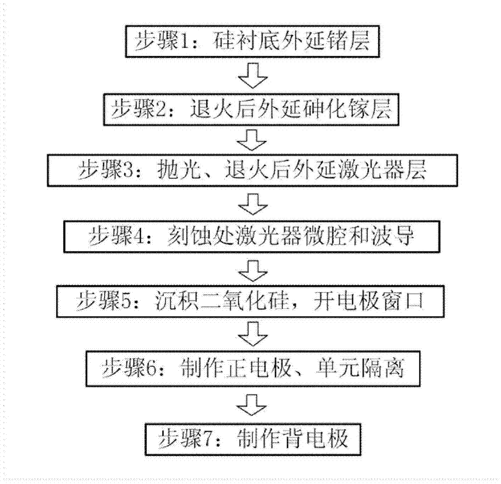
[0029] In order to make the object, technical solution and advantages of the present invention clearer, the present invention will be further described in detail below in conjunction with specific embodiments and with reference to the accompanying drawings.

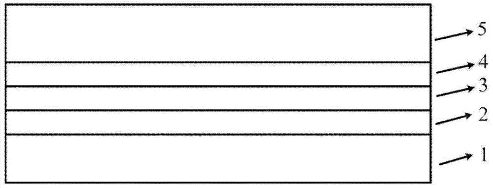
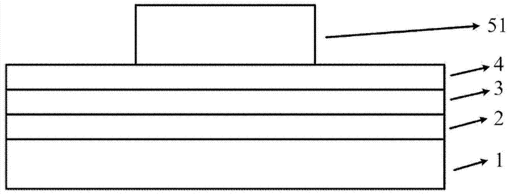
[0030] figure 1 A flow chart of a fabrication method of a silicon-based microcavity laser proposed by the present invention is shown. Figure 2-8 A process flow chart of manufacturing a silicon-based microcavity laser according to the above-mentioned method proposed by the present invention is shown. Such as Figure 1-8 Shown, this preparation method comprises the following steps:

[0031] Step 1: on the front side of the silicon substrate 1, an epitaxial germanium layer 2 is adopted by an ultra-high vacuum chemical vapor deposition method;

[0032] Step 2: Immediately put the silicon substrate 1 with the germanium layer 2 epitaxially into the MOCVD reaction chamber, and grow the low-temperature nucleated gallium arsen...


PUM

PropertyMeasurementUnit
surface roughnessaaaaaaaaaa
thicknessaaaaaaaaaa
surface roughnessaaaaaaaaaa

Abstract

The invention discloses a method for manufacturing a silicon substrate microcavity laser device. The method for manufacturing the silicon substrate microcavity laser device comprises the steps that a germanium layer is formed on the front face of a silicon substrate in an extension mode by adopting an ultra-high vacuum chemical vapor deposition method; the silicon substrate with the epitaxial germanium layer is put in an MOCVD reaction chamber, and a low-temperature nucleary gallium arsenide layer and a high-temperature gallium arsenide layer are grown in sequence respectively; a laser device structure is formed in an extension mode after surface polishing is carried out on the high-temperature gallium arsenide layer; a mocrocavitie and an output waveguide are formed on the laser device structure in a drying etching mode; a silicon dioxide layer is deposited after the mocrocavitie and the output waveguide are formed, and an electrode window is formed in the upper portion of the microcavity; positive electrodes are manufactured on the silicon dioxide layer and the upper surface of the electrode window, and electrode isolation is carried out; a back electrode is manufactured on the back face of the silicon substrate, and the manufacturing of the device is completed. According to the method for manufacturing the silicon substrate microcavity laser device, high-quality III-V group layers are achieved by combining the ultra-high vacuum chemical vapor phase epitaxy and MOCVD, and the cleanness and leveling of the surface are achieved by polishing and cleaning. The smooth side wall of the microcavity is achieved through drying etching and wet etching, and the losses of the laser device are reduced.

Description

technical field [0001] The invention relates to the field of semiconductor substrates, in particular to a method for manufacturing a silicon-based microcavity laser, which is used to combine ultra-high vacuum chemical vapor deposition and MOCVD to manufacture a silicon-based microcavity laser, which is applied to silicon-based optoelectronic integration and silicon-based photonics. Background technique [0002] For half a century, as the material basis of microelectronics technology, semiconductor silicon has promoted the rapid development of modern information technology. "When the price remains unchanged, the number of transistors that can be accommodated on an integrated circuit will increase by one every 18 months. times, the performance will also be doubled." The performance of integrated circuit chips has been greatly improved, and it has brought huge economic benefits; however, when the transistor feature size is gradually reduced, the production cost has also begun t...

Claims


Application Information

Patent Timeline
Patent Type & Authority Applications(China)
IPC IPC(8): H01S5/323H01S5/10
Inventor 周旭亮于红艳李梦珂潘教青王圩
Owner INST OF SEMICONDUCTORS - CHINESE ACAD OF SCI
Why Eureka
Try Eureka