
Formation method of semiconductor structure

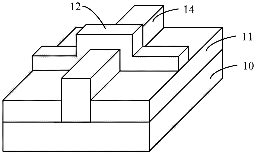
A semiconductor and gate structure technology, applied in the field of semiconductor structure formation, can solve the problems of increasing the contact area between the gate structure and the fin, complex formation process, poor performance, etc., to suppress the short channel effect, increase the contact area, Create simple effects

Inactive Publication Date: 2014-02-19
SEMICON MFG INT (SHANGHAI) CORP
View PDF4 Cites 10 Cited by
  • Summary
  • Abstract
  • Description
  • Claims
  • Application Information

AI Technical Summary

Problems solved by technology

[0005] With the further shrinking of the process node, the short channel effect of the fin field effect transistor in the prior art is becoming more and more obvious, and the performance is poor; in order to further suppress the short channel effect of the fin field effect transistor, the prior art proposes a "Ω ""-shaped fin field effect transistor (Ω-fin FET); the fin of the "Ω"-shaped fin field effect transistor includes a first sub-fin and a second sub-fin located on the surface of the first sub-fin The sidewall of the first sub-fin is recessed into the fin, so that the width of the first sub-fin is smaller than the width of the second sub-fin, thereby increasing the contact area between the gate structure and the fin, so that Suppression of short channel effects
[0006] However, the formation process of the "Ω"-shaped fin field effect transistor in the prior art is complicated, which is not conducive to popularization

Method used


Image

  • Formation method of semiconductor structure
  • Formation method of semiconductor structure
  • Formation method of semiconductor structure

Examples


Embodiment Construction

[0033] As mentioned in the background art, the formation process of the “Ω”-shaped fin field effect transistor in the prior art is complicated, which is not conducive to popularization.

[0034] specifically, Figure 2 to Figure 6 It is a schematic cross-sectional structure diagram of the formation process of an "Ω"-shaped fin field effect transistor in the prior art.

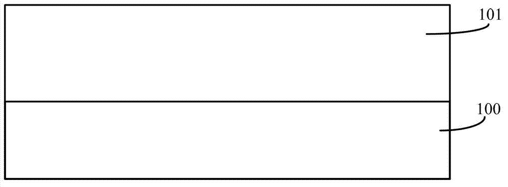
[0035] Please refer to figure 2 , providing a semiconductor substrate 100 with a fin layer 101 on the surface of the semiconductor substrate 100 .

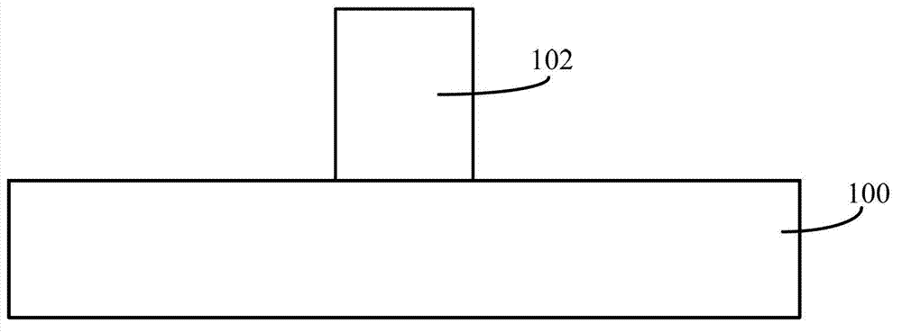
[0036] Please refer to image 3 , etch the fin layer 101 to form the fin 102 .

[0037] Please refer to Figure 4 , forming an insulating layer 103 covering part of sidewalls of the fins 102 on the surface of the semiconductor substrate 100 .

[0038] Please refer to Figure 5 A mask layer 104 is formed on the surface of the insulating layer 103 and the sidewall and top surface of the fin 102 .

[0039] Please refer to Figure 6 , remove the insulating lay...


PUM

PropertyMeasurementUnit
Thicknessaaaaaaaaaa
Thicknessaaaaaaaaaa

Abstract

A formation method of a semiconductor structure comprises: providing a semiconductor substrate, wherein the surface of the semiconductor substrate is provided with mask layers, and the semiconductor substrate is internally provided with mutually-isolated first openings; forming protection layers on the side walls of the first openings; with the protection layers and the mask layers being as a mask, utilizing anisotropic dry etching process to etch the bottoms of the first openings and thus second openings are formed; etching the side walls of the second openings so as to enable the side walls of the second openings to sunken into the semiconductor substrate; and after etching the side walls of the second openings, removing the protection layers and the mask layers, and thus a fin portion are formed on the semiconductor substrate between each first opening and each second opening. The formation process of the semiconductor structure is simple, and cost is saved.

Description

technical field [0001] The invention relates to the technical field of semiconductor manufacturing, in particular to a method for forming a semiconductor structure. Background technique [0002] With the rapid development of semiconductor manufacturing technology, semiconductor devices are developing towards higher element density and higher integration. Transistors, as the most basic semiconductor devices, are currently being widely used. Therefore, as the component density and integration of semiconductor devices increase, the gate size of transistors is also getting shorter and shorter. However, the shortening of the gate size of the transistor will cause the short-channel effect of the transistor, thereby generating leakage current, and ultimately affecting the electrical performance of the semiconductor device. [0003] In order to overcome the short channel effect of the transistor and suppress the leakage current, the prior art proposes a fin field effect transistor ...

Claims


Application Information

Patent Timeline
IPC IPC(8): H01L21/336H01L29/78
CPCH01L29/7853H01L29/66795H01L29/1033
Inventor 焦明洁刘佳磊
Owner SEMICON MFG INT (SHANGHAI) CORP
Learn More