Method for manufacturing circuit board

A production method and circuit board technology, which is applied in the fields of printed circuit manufacturing, printed circuit, electrical components, etc., can solve the problems of high labor and equipment investment costs, water, air environmental pollution, and human harm, and achieve simple production and reduce Wet process, the effect of reducing environmental pollution

Inactive Publication Date: 2014-02-19
丁保美
View PDF3 Cites 1 Cited by
  • Summary
  • Abstract
  • Description
  • Claims
  • Application Information

AI Technical Summary

Problems solved by technology

[0003] The existing circuit board processing technology includes the following steps: copper-clad substrate drilling—cleaning (deburring, grinding)—copper sinking—film—alignment—exposure and development (or anti-corrosion ink)—graphic plating—etching—film removal —Electrical continuity detection—cleaning treatment—screen printing solder mask pattern (printing green oil)—curing—screen printing mark symbols, etc., the whole process requires at least fifteen steps, and the process is quite complicated, requiring labor input and equipment The input cost is quite large. In addition, at least eight of the above-mentioned processes are wet processes. These wet processes often use some substances for cleaning, such as formaldehyde. On the other hand, it has caused serious environmental pollution to water, air, etc.

Method used


Image

  • Method for manufacturing circuit board

Examples


Embodiment Construction

[0027] The technical solution of the present invention will be described in detail below in conjunction with the accompanying drawings and specific embodiments, so as to understand the essence of the present invention more clearly and intuitively.

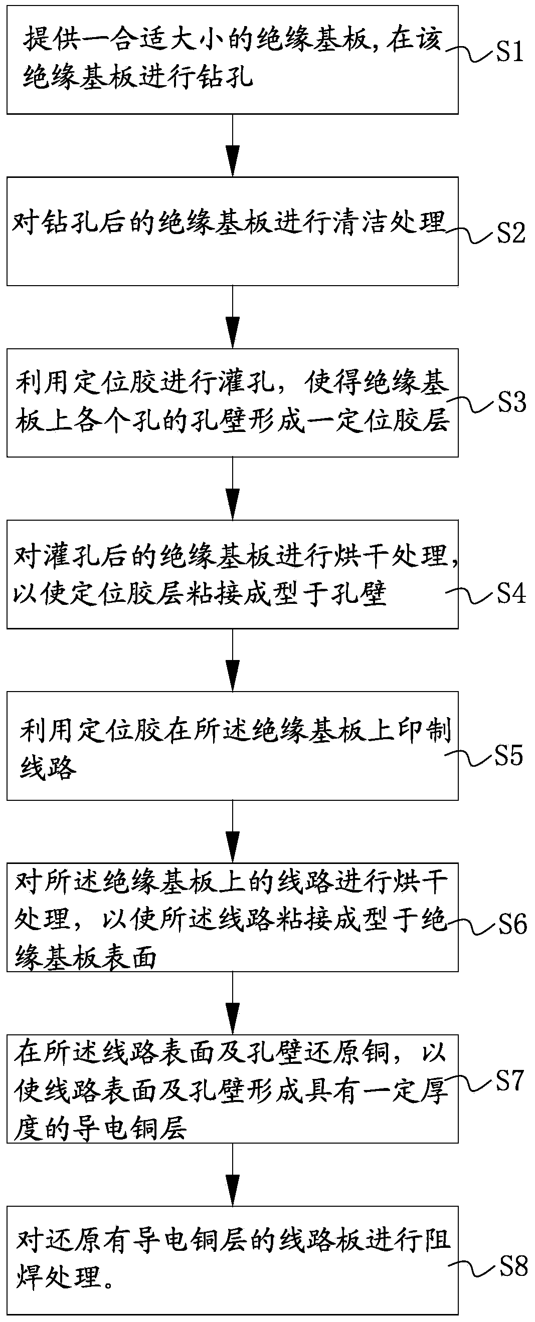
[0028] refer to figure 1 As shown, the invention provides a kind of manufacturing method of circuit board, and it comprises the following steps:

[0029] S1. Provide an insulating substrate of a suitable size, and drill holes in the insulating substrate; in this step, the substrate is directly used as an insulating substrate, generally a commonly used glass fiber board, and the insulating substrate is a substrate without copper clad. It is different from the copper-clad substrate in the prior art.

[0030] S2. Clean the insulating substrate after drilling; this step is the same as the existing process, which is a wet process, that is, using mechanical pressure and high-pressure water to scrub and rinse the board surface and foreig...


PUM


Abstract

The invention relates to a method for manufacturing a circuit board. The method comprises the steps of providing an insulation substrate, drilling a hole in the insulation substrate, carrying out cleaning treatment, filling the hole with locating and reduction glue to enable a locating and reduction glue layer to be formed on the wall of the hole, drying the insulation substrate with the hole filled, printing a circuit on the insulation substrate through the locating and reduction glue, drying the circuit, carrying out copper reduction on the surface of the circuit and the wall of the hole to enable conduction copper layers to be formed on the surface of the circuit and the wall of the hole and carrying out resistance welding on the circuit board. Hole filling and circuit printing are carried out on the insulation substrate through the locating and reduction glue, then the copper layer is restored on the circuit and the wall of the hole, and compared with the prior art, the method eliminates the steps of copper plating, film pasting, alignment, exposure development, etching and film removal which must be carried out when a copper-coated substrate is manufactured, greatly simplifies process steps, and is higher in efficiency. Meanwhile, invested cost of manpower and mechanical equipment is lowered, and the method saves more energy and is more environmentally friendly.

Description

technical field [0001] The invention relates to the technical field of circuit board processing, in particular to a method for manufacturing a circuit board which is simpler, environment-friendly and energy-saving compared with traditional methods. Background technique [0002] Circuit boards (including PCB and FPC) are circuit carriers in electronic products, and electronic products are an indispensable necessity in the information age. Therefore, it is determined that the circuit board processing industry is an indispensable industry in economic development, and it is also a high Pollution, high energy consumption and high cost industries. [0003] The existing circuit board processing technology includes the following steps: copper-clad substrate drilling—cleaning (deburring, grinding)—copper sinking—film—alignment—exposure and development (or anti-corrosion ink)—graphic plating—etching—film removal —Electrical continuity detection—cleaning treatment—screen printing sold...

Claims


Application Information

Patent Timeline
Patent Type & Authority Applications(China)
IPC IPC(8): H05K3/00
Inventor 丁保美
Owner 丁保美
Why Eureka
Try Eureka