
Eureka
For R&D, Eureka makes reading and utilizing patents & technical documents easy.
Eureka AIR
Designed for self-driven R&D workflows. Generate viable solutions, solve complex R&D challenges, empower your innovation with AI.

Eureka Materials
Designed for material experts only. Revolutionize your material R&D, from search, analyze, to developing new materials.

TechResearch
Generate reliable direction feasibility study reports for your R&D in just a few steps.

TechSeek
Discover and master advanced knowledge NOW. Basics, ideas, possibilities, all at once.

TechMind
As an expert in R&D Theories, TechMind can generates customized viable solutions instantly.

TechRisk
Analyze your overall solution with one click, know your potential R&D risks in advance.

TechMonitor
Get weekly tech updates, stay abreast of the latest tech innovations and key insights.
Electrostatic discharge resistant LDMOS device
An antistatic and device technology, applied in the electronic field, can solve problems such as damage, uneven opening of parasitic BJTs, current concentration, low ESD performance, etc., achieve process compatibility and improve ESD capabilities
- Summary
- Abstract
- Description
- Claims
- Application Information
AI Technical Summary
Problems solved by technology
Method used
Image

Examples
Embodiment Construction
[0019] In order to make the technical problems, technical solutions and positive effects to be solved by the present invention clearer, the present invention will be further described in detail below in conjunction with the accompanying drawings.
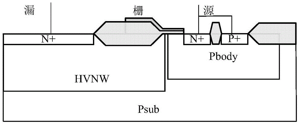
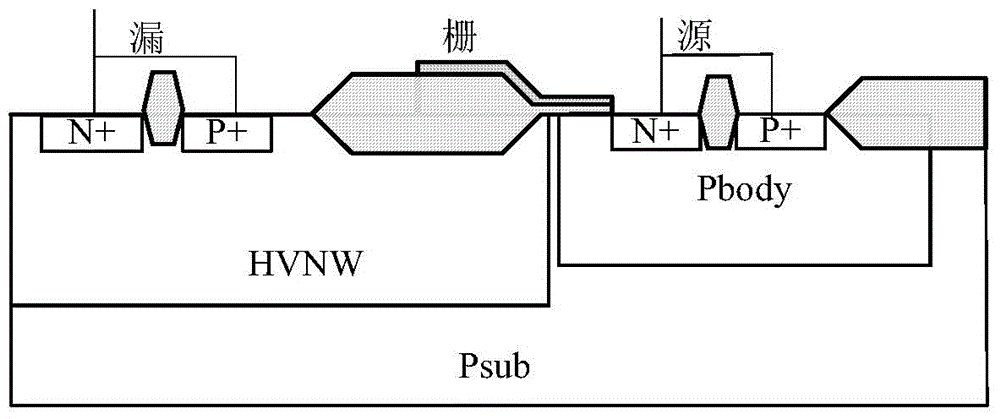
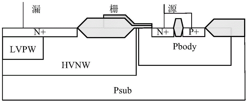
[0020] An anti-static discharge LDMOS device such as image 3 As shown, a conventional LDMOS device is included; the conventional LDMOS device includes a P-type semiconductor substrate, a P-type semiconductor base region and an N-type semiconductor drift region located on the surface of the P-type semiconductor substrate, and the P-type semiconductor base region and N Type semiconductor drift regions are independent of each other and do not contain each other; there are N+ source regions and P+ contact regions that are independent of each other and do not contain each other on the surface of the P-type semiconductor base region, wherein the N+ source region is close to the N-type semiconductor drift region and the P+ contact region ...
PUM
 Abstract
Description
Claims
Application Information
 - R&D Engineer
- R&D Manager
- IP Professional
- Industry Leading Data Capabilities
- Powerful AI technology
- Patent DNA Extraction
Browse by: Latest US Patents, China's latest patents, Technical Efficacy Thesaurus, Application Domain, Technology Topic, Popular Technical Reports.
© 2024 PatSnap. All rights reserved.Legal|Privacy policy|Modern Slavery Act Transparency Statement|Sitemap|About US| Contact US: help@patsnap.com