Film passivation structure for crystalline silica solar cell

A technology of solar cells and crystalline silicon, applied in circuits, photovoltaic power generation, electrical components, etc., can solve problems such as unsatisfactory passivation effects

Inactive Publication Date: 2014-02-26
TRINA SOLAR CO LTD
View PDF7 Cites 5 Cited by
  • Summary
  • Abstract
  • Description
  • Claims
  • Application Information

AI Technical Summary

Problems solved by technology

[0003] The passivation film on the front surface refers to the passivation film attached to the light-receiving surface of the cell. The surface oxidation passivation film commonly used includes silicon oxide film, hydrogenated amorphous microcrystalline silicon film and silicon nitride film. For example, the patent number is CN201655813 U The passi...

Method used


Image

  • Film passivation structure for crystalline silica solar cell

Examples


Embodiment Construction

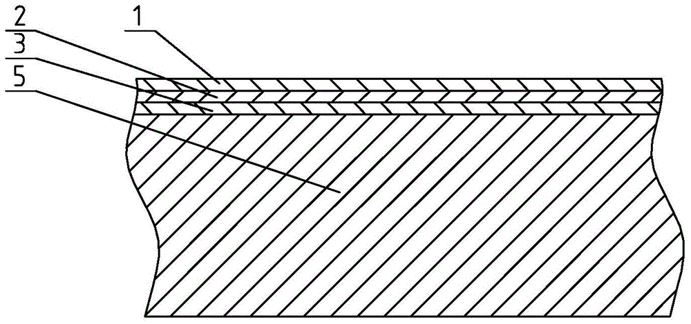
[0012] In order to make the content of the present invention easier to understand clearly, the present invention will be described in further detail below according to specific embodiments in conjunction with the accompanying drawings,

[0013] Such as figure 1 Shown, a kind of thin film passivation structure of crystalline silicon solar cell, it comprises SiNx thin film layer 1, aluminum oxide thin film layer 2 and grows on the p-type doped layer of silicon chip substrate 5 front or backside The silicon thin film layer 3 and the aluminum oxide thin film layer 2 are grown on the outer surface of the silicon dioxide thin film layer 3 , and the SiNx thin film layer 1 is grown on the outer surface of the aluminum oxide thin film layer 2 .

[0014] SiN x The refractive index of the thin film layer 1 is 1.9-2.4, the refractive index of the aluminum oxide thin film layer 2 is 1.55-1.65, and the refractive index of the silicon dioxide thin film layer 3 is 1.4-1.5. Because of the ef...


PUM

PropertyMeasurementUnit
Thicknessaaaaaaaaaa
Thicknessaaaaaaaaaa

Abstract

The invention discloses a film passivation structure for a crystalline silica solar cell. The film passivation structure comprises a SiNx film layer, an alumina film layer, and a silicon dioxide film layer growing on the P-type doping layer on front surface or back surface of a silicon chip substrate, wherein the alumina film layer grows on the outer surface of the silicon dioxide film layer, and the SiNx film layer grows on the outer surface of the alumina film layer. The film passivation structure for the crystalline silica solar cell can effectively passivate the P-type doping surface of a silicon chip and form good interface passivation effects.

Description

technical field [0001] The invention relates to a film passivation structure of a crystalline silicon solar cell, belonging to the technical field of crystalline silicon solar cells. Background technique [0002] At present, surface passivation can reduce the surface activity of cells and reduce the recombination rate of the surface. Currently, there are generally two measures for surface passivation of solar cells, namely surface oxidation passivation and transmitter passivation. The mechanism of surface oxidation passivation is to saturate the dangling bonds on the silicon surface and reduce the surface minority carrier recombination center. The common method is to grow a layer of silicon oxide or silicon nitride film on the surface of the cell; the mechanism of emitter passivation is to The surface is doped with a high concentration of impurities. In a very thin surface layer, the drift electric field directed to the inside of the silicon wafer is formed due to the impuri...

Claims


Application Information

Patent Timeline
IPC IPC(8): H01L31/0216
CPCH01L31/02167Y02E10/50
Inventor 盛健张淳
Owner TRINA SOLAR CO LTD
Why Eureka
Try Eureka