A back-contact crystalline silicon solar cell, its preparation method, component, and system

A technology for solar cells and crystalline silicon, applied in the field of solar cells, can solve problems such as being difficult to obtain, and achieve the effects of increasing open-circuit voltage and short-circuit current, reducing recombination, and excellent field passivation effect.

Active Publication Date: 2019-01-11
TAIZHOU ZHONGLAI PHOTOELECTRIC TECH CO LTD
View PDF3 Cites 0 Cited by
  • Summary
  • Abstract
  • Description
  • Claims
  • Application Information

AI Technical Summary

Problems solved by technology

In the prior art, the surface concentration of the front surface field obtained by diffusion by depositing a phosphorus source on the surface of the silicon wafer is generally 1E 19 cm -3 above, it is difficult to get a lower J 0 value

Method used


Image

  • A back-contact crystalline silicon solar cell, its preparation method, component, and system
  • A back-contact crystalline silicon solar cell, its preparation method, component, and system
  • A back-contact crystalline silicon solar cell, its preparation method, component, and system

Examples


Embodiment Construction

[0035] The present invention will be described in detail below in conjunction with the embodiments and the accompanying drawings. It should be noted that the described embodiments are only intended to facilitate the understanding of the present invention, rather than limiting it in any way.

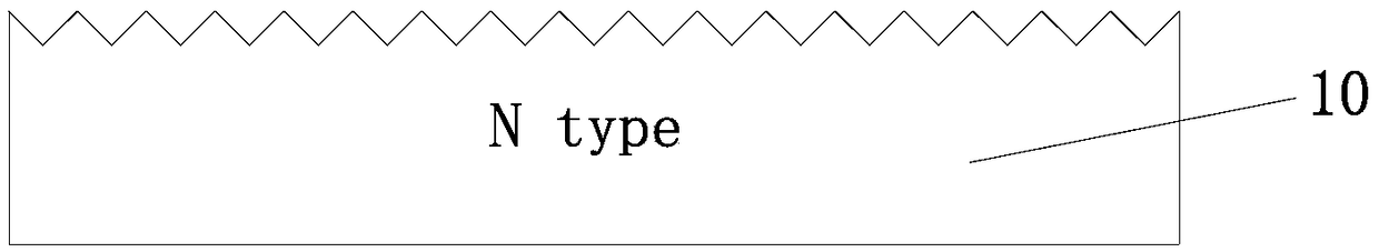
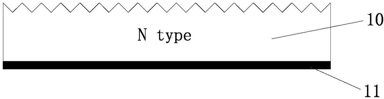
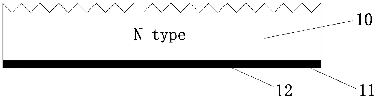
[0036] see Figure 7As shown, a back-contact crystalline silicon solar cell of this embodiment includes an N-type crystalline silicon substrate 10, and the front surface of the N-type crystalline silicon substrate 10 is an oxide layer on the front surface and an n+ doped polysilicon on the front surface. Layer 13 and anti-reflection film on the front surface; the back surface of the N-type crystalline silicon substrate 10 is sequentially composed of doped regions, passivation films on the back surface, and metal electrodes in ohmic contact with the doped regions, and the doped regions include alternately The back surface n+ doped region 12 and the back surface p+ doped region 11 are arran...


PUM


Abstract

The invention relates to a back contact crystalline silicon solar cell, a preparation method, a component and a system. The back contact crystalline silicon solar cell provided by the invention comprises a N type crystalline silicon substrate, wherein a front surface oxide layer, a front surface n+ doped polycrystalline silicon layer and a front surface antireflection coating are successively arranged on the front surface of the N type crystalline silicon substrate from inner to outer; a rear surface p+ doped area, a rear surface n+ doped area, a rear surface passivation coating and a rear surface metal electrode which are alternately arrayed are successively arranged on the rear surface of the N type crystalline silicon substrate from inner to outer. The back contact crystalline silicon solar cell has the beneficial effects that the n+ doped polycrystalline silicon layer is taken as a front surface field of the back contact crystalline silicon solar cell, an excellent field passivation effect is supplied to the surface of the N type crystalline silicon substrate, the compound of minority carriers on the front surface is reduced, the open-circuit voltage and short-circuit voltage of the back contact crystalline silicon solar cell are increased and the energy exchange efficiency is increased.

Description

technical field [0001] The invention relates to the technical field of solar cells, in particular to a back-contact crystalline silicon solar cell, a preparation method, an assembly, and a system. Background technique [0002] A solar cell is a semiconductor device that converts light energy into electrical energy. Lower production costs and higher energy conversion efficiency have always been the goals pursued by the solar cell industry. For conventional solar cells, the p+ doped region contact electrodes and the n+ doped region contact electrodes are respectively located on the front and back sides of the battery sheet. The front of the battery is the light-receiving surface, and the coverage of the metal contact electrodes on the front will inevitably cause a part of the incident sunlight to be blocked and reflected by the metal electrodes, resulting in a part of optical loss. The coverage area of ​​the front metal electrode of an ordinary crystalline silicon solar cell ...

Claims


Application Information

Patent Timeline
Patent Type & Authority Patents(China)
IPC IPC(8): H01L31/0216H01L31/18H01L31/048
CPCH01L31/02167H01L31/048H01L31/1804Y02E10/547Y02P70/50
Inventor 林建伟季根华刘志锋孙玉海刘勇张育政
Owner TAIZHOU ZHONGLAI PHOTOELECTRIC TECH CO LTD
Why Eureka
Try Eureka