Method for producing circuit board thin plates

A production method and circuit board technology, applied in printed circuit, printed circuit manufacturing, electrical components, etc., can solve the problems that tools cannot meet production requirements, thin plates are easy to be bent, and board surfaces are scratched, so as to improve the efficiency of electrical testing, Prevent stuck and broken boards, and avoid the effect of inserting wrong slots

Active Publication Date: 2014-03-05
广东依顿电子科技股份有限公司
View PDF4 Cites 18 Cited by
  • Summary
  • Abstract
  • Description
  • Claims
  • Application Information

AI Technical Summary

Problems solved by technology

The manufacturing quality of printed circuit boards not only directly affects the reliability of electronic products, but also affects the overall competitiveness of system products
[0003] The thickness of circuit board thin board is usually less than 0.28mm. If the production method of thick board is adopted in the past, many problems will occur, resulting in the scrapping of products in batches.
For example, the horizontal production line of printed circuit boards is prone to board jams and broken boards when conveying thin boards; when the graphics are transferred or the solder mask oil process is exposed, the board surface is scratched due to the lack of suitable transfer inserts during the transportation process; During graphic electroplating, the thin plate is too thin and easy to be clamped, which will cause the tank to fall off. The thin plate is easily bent during electroplating, causing the plate not to enter the floating frame, resulting in abnormal thickness of electroplated copper and scratching of the dry film or tin surface on the floating frame; in the electrical test, Due to the small size of the gong room and packaging process, the customer has higher requirements for packaging, and the existing production process and tools cannot meet the production problems.

Method used


Image

  • Method for producing circuit board thin plates
  • Method for producing circuit board thin plates
  • Method for producing circuit board thin plates

Examples


Embodiment Construction

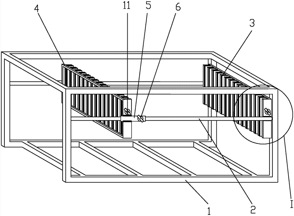
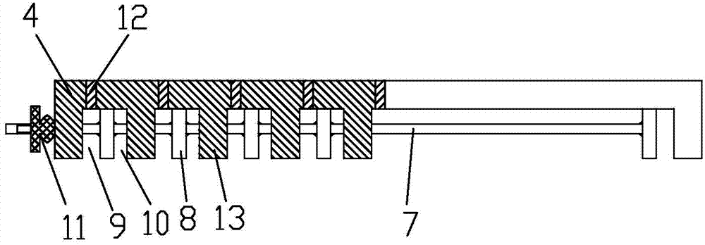
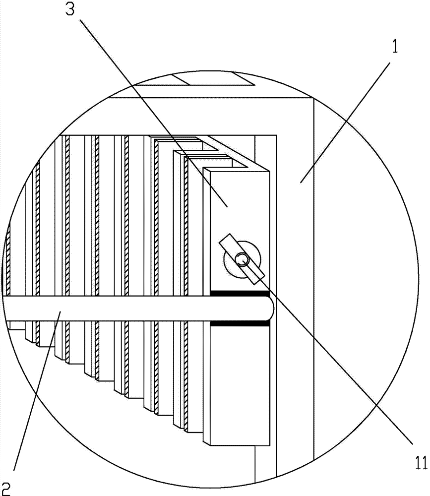
[0047] Below in conjunction with accompanying drawing, the present invention will be further described, and the operation of making circuit board sheet is as follows:

[0048] A) Cutting: Cutting the qualified raw material board is composed of copper clad laminate and resin film, cleaning and drying the surface;

[0049] B) Transfer of inner layer circuit pattern and circuit inspection: paste a layer of photosensitive material on the copper foil on the surface of the above circuit board, then carry out counter-position exposure through black film, form a circuit pattern after development, drill pipe position holes on the edge of the board, and Automatic optical detection equipment is used to detect whether there is a broken line or a short circuit on the circuit board surface;

[0050] C) Browning and pressing board: roughen the copper surface and wire surface as the inner layer; arrange the above-mentioned raw material boards according to the design requirements, and press th...


PUM


Abstract

The invention discloses a method for producing circuit board thin plates. The technical scheme is characterized in that the method comprises the following steps that: conducting plating though holes; conducting outer layer circuit pattern transfer; conducting graph electric plating and etching; penetrating a string through locating holes of the circuit board thin plates, utilizing string beads to separate the circuit board thin plates, and plating the circuit board thin plates though the holes, after plating the circuit board thin plates through the holes, washing liquid medicine on the surfaces of the circuit board thin plates away by horizontally drawing the circuit board thin plates through a thick plate; conducting electric test; conducting routing; utilizing a plastic package tray to package a finished-product unit plate subjected to routing. From the procedure of layer circuit pattern transferring to the procedure of routing, the circuit board thin plates are compressed through pressing grooves by the adoption of a pig cage frame device to be transferred between the procedures. The method for producing the circuit board thin plate solves the problems that the circuit board thin plates are prone to plate adhesion, plate curving, plate clamping and plate fracture due to the fact that the circuit board thin plates are small in size. The method for producing circuit board thin plates is simple in process and stable in product quality.

Description

【Technical field】 [0001] The invention relates to a production method of a circuit board sheet. 【Background technique】 [0002] With the rapid development of science and technology, circuit board sheets have received more and more attention. Consumers' requirements for ultra-thin and portable electronic products have provided opportunities for the development of circuit board sheets. While people enjoy the convenience of work and the improvement of the quality of life brought by high technology, the printed circuit board industry is also facing challenges in the fields of design, manufacturing and assembly due to the lightweight and miniaturization of electronic products. The manufacturing quality of printed circuit boards not only directly affects the reliability of electronic products, but also affects the overall competitiveness of system products. [0003] The thickness of the circuit board thin plate is usually less than 0.28mm. If the production method of the previous...

Claims


Application Information

Patent Timeline
Patent Type & Authority Applications(China)
IPC IPC(8): H05K3/00
Inventor 莫介云
Owner 广东依顿电子科技股份有限公司
Why Eureka
Try Eureka