Three-dimensional memory (3D-M) with integrated intermediate circuit chip

An intermediate circuit, three-dimensional storage technology, applied in circuits, electrical solid devices, electrical components, etc., can solve the problems of inability to reduce costs, increase costs, and troublesome intermediate circuit design.

Active Publication Date: 2014-03-12
CHENGDU HAICUN IP TECH
View PDF9 Cites 8 Cited by
  • Summary
  • Abstract
  • Description
  • Claims
  • Application Information

AI Technical Summary

Problems solved by technology

Since the three-dimensional memory array uses a complicated back-end process, and the back-end process of the intermediate circuit is relatively simple, the direct result of blindly integrating the intermediate circuit and the three-dimensional memory array is that the intermediate circuit has to be manufactured with the expensive process of manufacturing the three-dimensional memory array. circuit, which not only cannot reduce the cost, but will increase the cost
In addition, since the intermediate circuit can only use the same number of metal layers as the three-dimensional memory array (for example, only two layers), the design of the intermediate circuit is more troublesome, and the required chip area is larger.
On the other hand, since 3D-M storage elements generally undergo high-temperature processes, the intermediate circuit needs to use high-temperature-resistant interconnection materials, such as tungsten (W), which will degrade the overall performance of 3D-M

Method used


Image

  • Three-dimensional memory (3D-M) with integrated intermediate circuit chip
  • Three-dimensional memory (3D-M) with integrated intermediate circuit chip
  • Three-dimensional memory (3D-M) with integrated intermediate circuit chip

Examples


Embodiment Construction

[0027] In the present invention, " / " represents the relationship of "and" or "or". For example, a read / write voltage generator means that it can generate only read voltages, or only write voltages, or both read and write voltages; an address / data converter means that it can only convert addresses, or only data, or both Convert address and voltage.

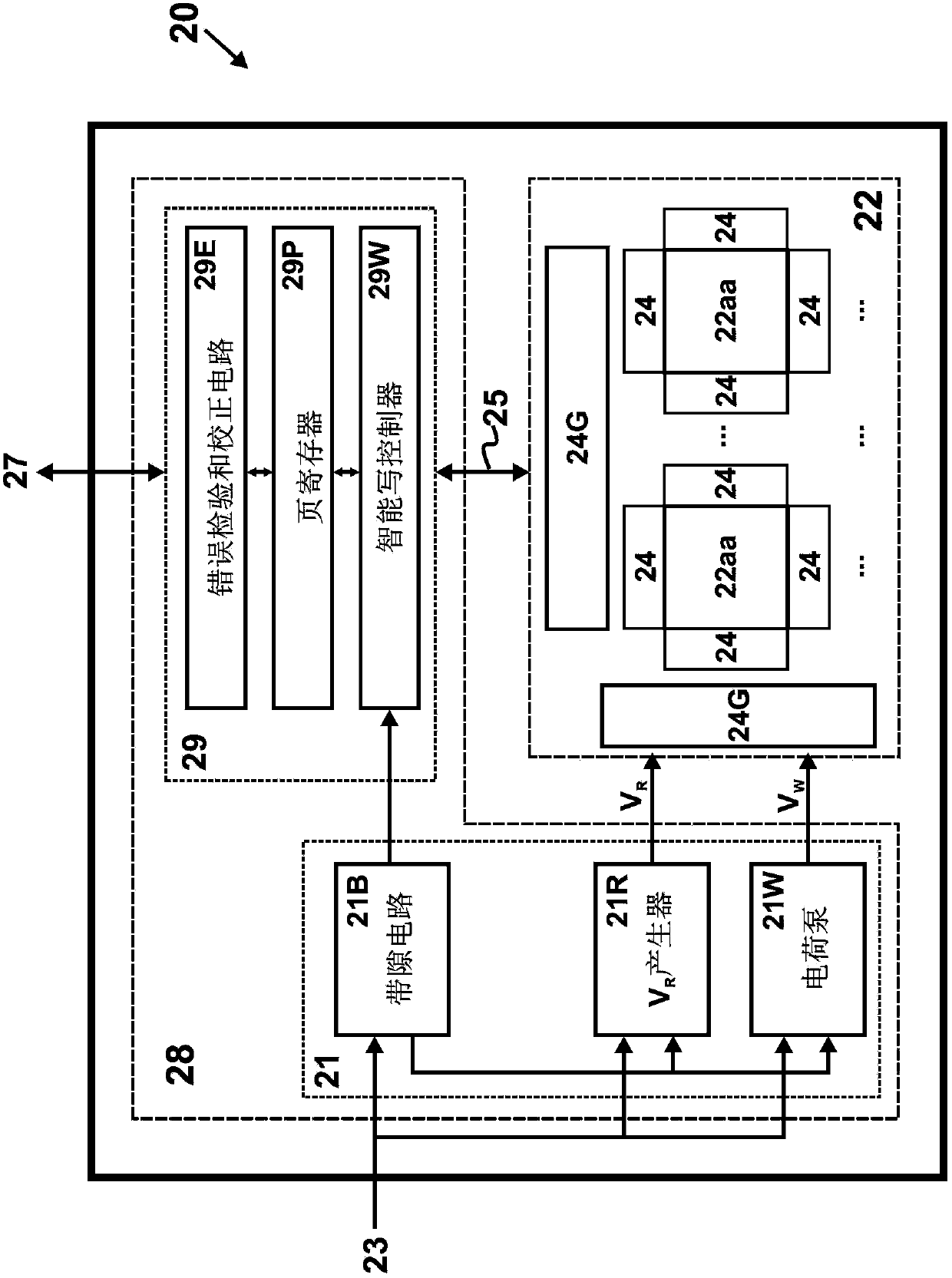
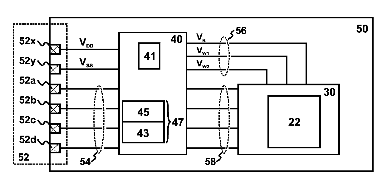
[0028] In the present invention, the intermediate circuit refers to a circuit between the 3D-M core area and the host, which implements voltage, address or / and data conversion between the host and the 3D-M core area. For example, it will come from an external voltage from the host (i.e. supply voltage V DD ), external address (that is, logical address) and external data (that is, logical data) are converted into the internal voltage of the 3D-M core area (that is, the read voltage V R and write voltage V W ), internal address (that is, physical address), and internal data (that is, physical data). Intermediate circuit component...


PUM


Abstract

The invention provides a 3D-M with an integrated intermediate circuit chip. The 3D-M comprises at least one independent 3D array chip and one intermediate circuit chip (40), wherein the intermediate circuit chip (40) comprises a reading / writing voltage generator (41) and an address / data converter (47), the reading / writing voltage generator (41) supplies at least one reading / writing voltage (VR / VW) different from a power supply voltage (VDD) for the 3D array chip (30), the address / data converter (47) mutually transforms address / data (54) of a host computer and address / data (58) of the 3D array chip (30), and the 3D array chip (30) is different from the intermediate circuit chip (40). The 3D-M can support multiple 3D array chips (30a, 30b...).

Description

technical field [0001] The present invention relates to the field of integrated circuit memories, more precisely three-dimensional memories (3D-M). Background technique [0002] Three-dimensional memory (3D-M) is a monolithic semiconductor memory that consists of multiple memory layers stacked on top of each other. 3D-M includes three-dimensional read-only memory (3D-ROM) and three-dimensional random access memory (3D-RAM). 3D-ROM can be further divided into three-dimensional mask programmed read-only memory (3D-MPROM) and three-dimensional electrically programmed read-only memory (3D-EPROM). Based on its programming mechanism, 3D-M can contain memristor, resistive random-access memory (RRAM or ReRAM), phase-change memory (PCM), programmable metallization memory (PMM), or conductive-bridging random-access memory (CBRAM). [0003] US Patent No. 5,835,396 discloses a 3D-M, namely 3D-ROM. As shown in FIG. 1A , the 3D-M chip 20 includes a substrate layer OK and a plurality of...

Claims


Application Information

Patent Timeline
IPC IPC(8): H01L27/10G06F11/10
CPCH01L24/06H01L2224/48091H01L2924/181
Inventor 张国飙
Owner CHENGDU HAICUN IP TECH
Why Eureka
Try Eureka