Test method and test system for LED wafer

A test method and wafer technology, applied in semiconductor/solid-state device testing/measurement, electrical components, circuits, etc., can solve the error of LED wafer Mapping full measurement value, affect the production cycle, consume labor and material costs, etc. problems, to achieve the effect of improving production efficiency and product yield, and solving the problem of abnormal control lag

Inactive Publication Date: 2014-03-19
西安利科光电科技有限公司
View PDF4 Cites 9 Cited by
  • Summary
  • Abstract
  • Description
  • Claims
  • Application Information

AI Technical Summary

Problems solved by technology

This approach not only occupies a large amount of testing machine capacity, but also consumes the manpower and material costs involved in testing machine calibration or monitoring.
And for a long time, the consistency problem of the testing machine has brought large errors to the full measureme

Method used


Image

  • Test method and test system for LED wafer
  • Test method and test system for LED wafer
  • Test method and test system for LED wafer

Examples


Embodiment Construction

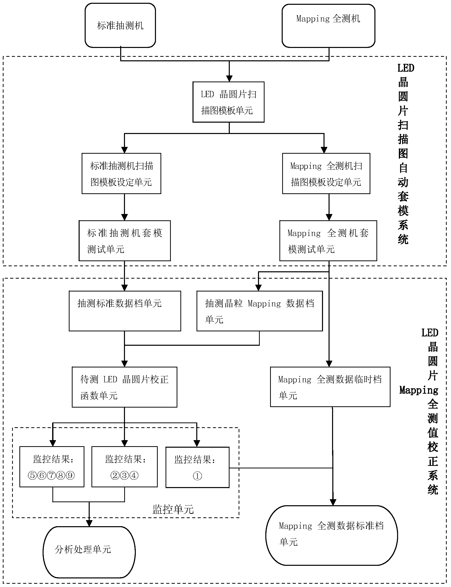
[0059] First the parameters involved in the implementation steps of the present invention are described as follows:

[0060] WL.offset: the wavelength correction function after differentiation;

[0061] IV.gain: Light intensity correction function after differentiation;

[0062] WL.std: When the LED wafer to be tested is sampled by the standard sampling machine, the wavelength value of the grain is sampled;

[0063] IV.std: When the LED wafer to be tested is sampled by a standard sampling machine, the light intensity value of the grains is sampled;

[0064] WL.smap: the wavelength value of sampling grains tested on the Mapping full testing machine;

[0065] IV.smap: Sampling the light intensity value of the crystal grains tested by the Mapping full testing machine;

[0066] WL.map: the initial wavelength value of the LED wafer to be tested in the Mapping full test machine;

[0067] IV.map: The initial light intensity value of the LED wafer to be tested in the Mapping full ...


PUM


Abstract

The invention provides a test method and a test system for an LED wafer. The test system includes a standard spot-test machine, an LED wafer scintigram template unit, a standard spot-test machine scintigram template setting unit, a standard spot-test machine cover-die test unit, a spot-test standard data file unit, a to-be-tested LED wafer correction function unit, a monitoring unit and an analyzing processing unit, which are connected sequentially. A Mapping full-test machine, the LED wafer scintigram template unit, a Mapping full-test machine scintigram template setting unit, a Mapping full-test cover machine cover-die test unit and a Mapping full-test data temporary file unit, which are sequentially connected, are connected with a Mapping full-test data standard file unit sequentially. The Mapping full-test machine cover-die test unit is connected with the to-be-tested LED wafer correction function unit through a spot-test grain Mapping data file unit. The monitoring unit is connected with the Mapping full-test data standard file unit. The test method and test system for the LED wafer derates personnel and material costs related with Mapping full-test machine correction and monitoring and at the same time, improves machine productivity use rate and reduces the manufacturing cost of the LED wafer.

Description

technical field [0001] The invention belongs to the field of LED chip manufacturing, in particular to an LED wafer testing method and testing system. Background technique [0002] The consistency of the optical parameters such as the wavelength and light intensity of the LED wafer in each Mapping full-test machine, the frequent calibration and monitoring workload of the Mapping full-test machine, and the hysteresis of abnormal monitoring have always been problems for LED chip manufacturers. one of the difficulties. At present, the common practice is to use LED standard samples (LED standard chip or standard packaging device) to calibrate or monitor the LED wafer testing machine one by one at intervals of several batches or a certain period of time, and confirm the mapping between the full testing machine and the standard testing machine. When the consistency meets the machine control requirements, the on-machine scanning of LED wafers and the full mapping of photoelectric p...

Claims


Application Information

Patent Timeline
IPC IPC(8): H01L21/66H01L33/00
CPCH01L22/12H01L22/14H01L22/20
Inventor 赖余盟陈起伟周立业缪炳有李斌
Owner 西安利科光电科技有限公司
Why Eureka
Try Eureka