High temperature resistance electronic device raw material and application thereof

A technology of electronic devices and raw materials, applied in the field of semiconductor materials, can solve the problems of device heat accumulation and temperature rise, deterioration of device electrical parameters, poor thermal conductivity of silicon dioxide, etc., and achieve stable threshold voltage and junction leakage current Effect of small, high breakdown electric field and electron saturation drift velocity

Inactive Publication Date: 2014-03-19
SHANDONG UNIV
View PDF8 Cites 0 Cited by
  • Summary
  • Abstract
  • Description
  • Claims
  • Application Information

AI Technical Summary

Problems solved by technology

Although the CMOS circuit with SOI structure (with silicon dioxide as the insulating buried layer) eliminates the latch-up effect excited at high temperature and has a small high-temperature leakage current, however, when working at high temperature downhole, due to the thermal conductivity of silicon dioxide Poor, the heat generated inside the device is difficult to dissipate, and there are self-heating effects and parasitic capacitance, which lead to heat accumulation and temperature rise of the device, resulting in deterioration of the electrical parameter characteristics of the device or even failure

Method used


Image

  • High temperature resistance electronic device raw material and application thereof
  • High temperature resistance electronic device raw material and application thereof
  • High temperature resistance electronic device raw material and application thereof

Examples


Embodiment 1

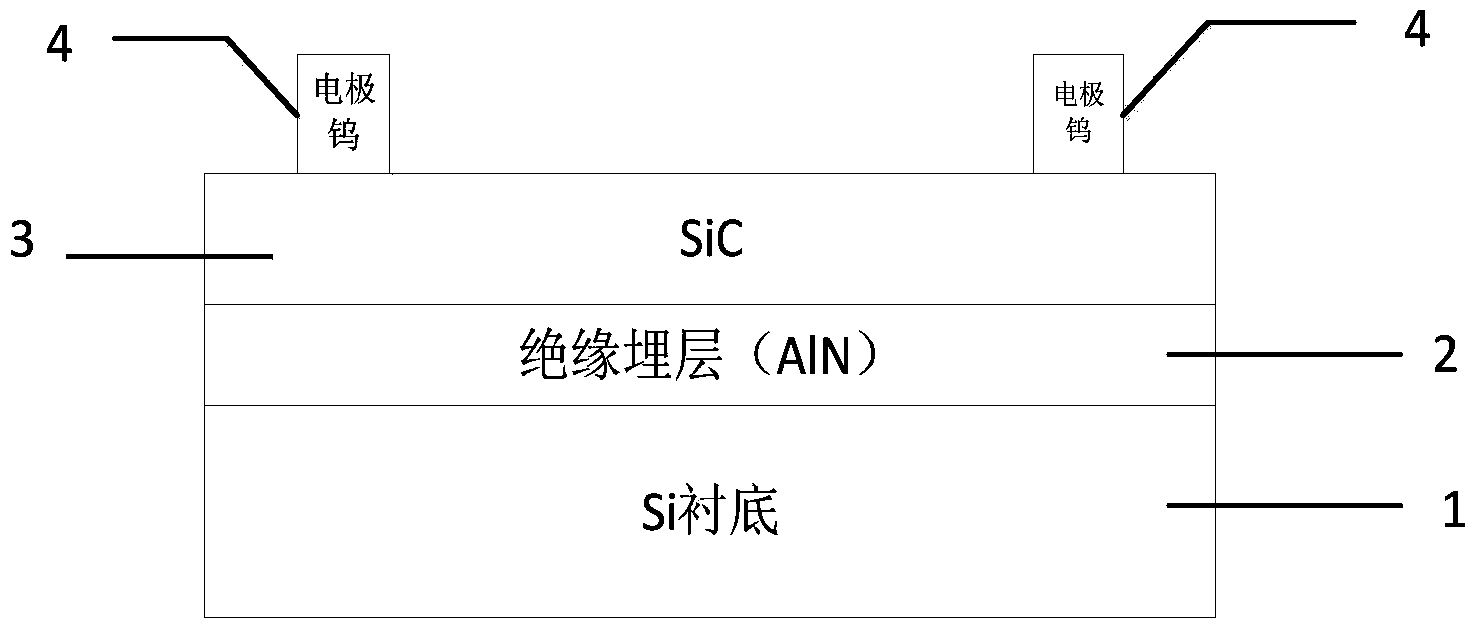
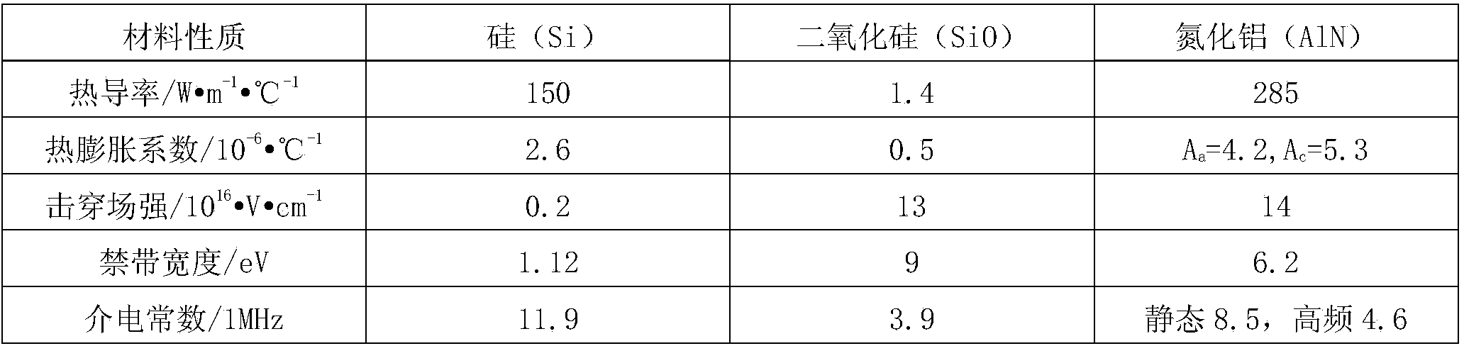
[0036] like figure 1 , figure 2 , Figure 5 and Image 6 As shown, a high temperature resistant electronic device material, the structure of the electronic device material includes a substrate layer 1, an insulating buried layer 2, a conductor layer 3 and an electrode 4, wherein the insulating buried layer 2 is arranged on the upper surface of the substrate layer 1, and the conductor The layer 3 is arranged on the upper surface of the insulating buried layer 2, the electrode 4 is arranged on the upper surface of the conductive layer, the material used for the substrate layer 1 is Si, the material used for the insulating buried layer 2 is AlN, and the material used for the conductive layer 3 is SiC. The material used for the motor 4 is tungsten, the thickness of the substrate layer is 1um, the thickness of the insulating buried layer is 0.1um, and the thickness of the conductor layer is 0.1um. figure 2 It shows that the material used for the insulating buried layer is AlN, S...

Embodiment 2

[0038] like figure 1 , Figure 5 and Image 6 As shown, a high temperature resistant electronic device material, its structure is as shown in Example 1, the difference is that the thickness of the conductor layer 3 is 0.3um.

Embodiment 3

[0040] like figure 1 , Figure 5 and Image 6 As shown, a high temperature resistant electronic device material, its structure is as shown in Example 1, the difference is that the thickness of the conductor layer 3 is 0.15um.


PUM


Abstract

The invention relates to a high temperature resistance electronic device raw material and application thereof and particularly relates to the raw material applied to an electronic device in an underground drilling tool circuit of a petroleum logging. A structure of the electronic device raw material comprises a substrate layer, an insulative buried layer, a conductor layer and an electrode, wherein the insulative buried layer is arranged at an upper surface of the substrate layer, the conductor layer is arranged at an upper surface of the insulative buried layer, the electrode is arranged at an upper surface of the conductor layer, the substrate layer employs a Si material, the insulative buried layer employs an AlN material, the conductor layer employs a SiC material, and the electrode employs a tungsten material. The high temperature resistance electronic device raw material prepared by employing SiCOI, silicon carbide at the insulative buried layer, can effectively avoid increase of leakage current, prevents a latch-up effect, further has a more stable threshold voltage under high temperature and is suitable for being selected as the raw material applied to the electronic device in the underground drilling tool circuit of the petroleum logging under a high temperature environment.

Description

technical field [0001] The invention relates to a high-temperature-resistant electronic device raw material and its application, and belongs to the technical field of semiconductor material application. Background technique [0002] With the continuous development of oil drilling technology, downhole drilling tools need to adapt to complex and harsh environments, especially devices and circuits that can work at high temperatures. At present, bulk silicon devices used in downhole drilling tool circuits cannot work in a high temperature environment above 250°C due to the increase of leakage current at high temperature, the drift of threshold voltage, and the thermally induced latch-up effect. Signals from sensors in high-temperature environments are transmitted to remote processors through wires or complex cooling systems are used to keep the processors on the equipment at an appropriate temperature. The former increases the length of wires and the number of joints, leading t...

Claims


Application Information

Patent Timeline
Patent Type & Authority Applications(China)
IPC IPC(8): H01L27/12H01L27/146
Inventor 李康王刚
Owner SHANDONG UNIV
Why Eureka
Try Eureka