Chip transfer method for LED (light-emitting diode) wafer level package

A wafer-level packaging, LED epitaxial wafer technology, applied in electrical components, circuits, semiconductor devices, etc., can solve the problems of high lattice mismatch, complicated process, poor thermal conductivity and electrical conductivity

Active Publication Date: 2014-03-19
INST OF SEMICONDUCTORS - CHINESE ACAD OF SCI
View PDF5 Cites 32 Cited by
  • Summary
  • Abstract
  • Description
  • Claims
  • Application Information

AI Technical Summary

Problems solved by technology

This chip manufacturing method needs to repeatedly install a single die, the process is complicated, affects the production speed, and the cost is difficult to reduce
In addition, in the current technology, the sapphire substrate is left on the chip, and there is a high lattice

Method used


Image

  • Chip transfer method for LED (light-emitting diode) wafer level package
  • Chip transfer method for LED (light-emitting diode) wafer level package
  • Chip transfer method for LED (light-emitting diode) wafer level package

Examples


Embodiment Construction

[0020] In order to make the object, technical solution and advantages of the present invention clearer, the present invention will be further described in detail below in conjunction with specific embodiments and with reference to the accompanying drawings.

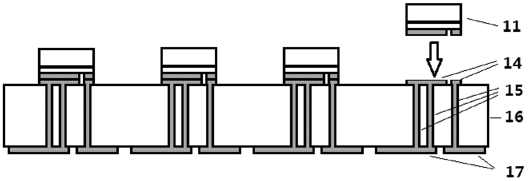
[0021] see Figures 2A-2F , a chip manufacturing method for wafer-level packaging of LEDs, comprising the steps of:

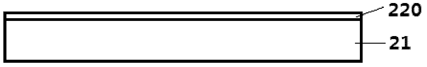
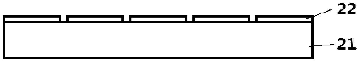
[0022] Such as Figure 2A , 2B As shown, the LED epitaxial wafer used is obtained by metal-organic chemical vapor deposition (MOCVD). On the sapphire substrate 21, a gallium nitride-based epitaxial film 220 is epitaxially grown. The gallium nitride-based epitaxial film 220 includes but is not limited to n-type nitride, active layer, p-type nitride. The epitaxial film 220 is fabricated into separate LED unit devices 22 through chip processes, mainly including cleaning, photolithography, etching, electrode fabrication, passivation, grinding and polishing, etc. Among them, the mesa is etched by ICP to exp...


PUM

PropertyMeasurementUnit
Thicknessaaaaaaaaaa
Thicknessaaaaaaaaaa

Abstract

A chip transfer method for LED (light-emitting diode) wafer level package includes the steps: manufacturing an LED unit device array on an LED epitaxial wafer, manufacturing metal layers on parts of unit devices of the unit device array to serve as middle metal layers in bonding, and forming a unit device array to be bonded; manufacturing metal patterns corresponding to electrodes of the unit device array to be bonded on the front surface of a base plate, forming heat conduction channels and electric conduction channels below the metal patterns, and connecting electrodes of an LED unit device with a metal bonding pad on the back surface of the base plate through the electric conduction channels; conversely mounting the unit device array to be bonded on the base plate in a bonding mode; finally, sequentially stripping the unit devices to be bonded in a laser stripping mode, separating the epitaxial layers of the unit devices to be bonded from a substrate, and forming a whole film LED array by the separated epitaxial layers and the base plate. The chip transfer method can be used for wafer level package of the LED devices, package efficiency is improved, and cost is reduced.

Description

technical field [0001] The invention relates to a method for manufacturing a chip, in particular to a method for manufacturing a chip used for wafer-level packaging of LEDs. Background technique [0002] Light-emitting diodes are a new generation of lighting sources, and their technological development has been vigorously promoted by various countries. The luminous brightness and reliability of light-emitting diodes have been greatly improved in recent years, and their application fields are becoming more and more extensive, especially in the general lighting application field with huge market potential. It is expected to replace traditional incandescent lamps and fluorescent lamps in the near future. [0003] The traditional packaging method of LED is mainly packaged on a single-component substrate, that is, firstly, the epitaxial wafer is made into a single die through the chip process, and then the single die is packaged on various shells to complete the LED package. Thi...

Claims


Application Information

Patent Timeline
IPC IPC(8): H01L33/48H01L21/683
CPCH01L21/67132
Inventor 梁萌杨华刘志强伊晓燕王军喜王国宏李晋闽
Owner INST OF SEMICONDUCTORS - CHINESE ACAD OF SCI
Why Eureka
Try Eureka