Array substrate, manufacturing method thereof and display device

A technology of an array substrate and a manufacturing method, which is applied in the display field, can solve the problems of affecting TFT performance, high cost, complicated process, etc., and achieves the effect of saving the manufacturing process flow and manufacturing cost, and reducing the number of times.

Active Publication Date: 2014-03-19
BOE TECH GRP CO LTD
View PDF9 Cites 4 Cited by
  • Summary
  • Abstract
  • Description
  • Claims
  • Application Information

AI Technical Summary

Problems solved by technology

[0004] Among them, the active layer is usually an oxide semiconductor material, that is, the formed TFT is OxideTFT, so an additional etching stopper layer 5 is needed to prevent the oxide semiconductor material from being damaged when the source and drain layers are etched, which affects the TFT. performance
Therefore, the fabrication of the above-mentioned AMOLED display device usually requires 7 times of mask process (mask) formation (gate, via hole on the gate insulating layer, active layer, via hole on the etch stop layer, source and drain layer, passivation layer Vias on the upper layer and pixel definition layer each mask), the process is complex and the cost is high

Method used


Image

  • Array substrate, manufacturing method thereof and display device
  • Array substrate, manufacturing method thereof and display device
  • Array substrate, manufacturing method thereof and display device

Examples


Embodiment Construction

[0049] The specific implementation manners of the present invention will be further described in detail below in conjunction with the accompanying drawings and embodiments. The following examples are used to illustrate the present invention, but are not intended to limit the scope of the present invention.

[0050] The method for manufacturing an array substrate according to an embodiment of the present invention includes the following steps:

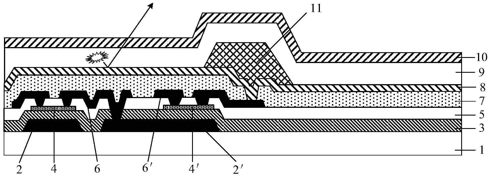
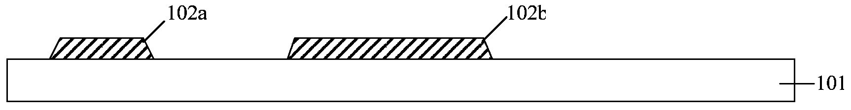
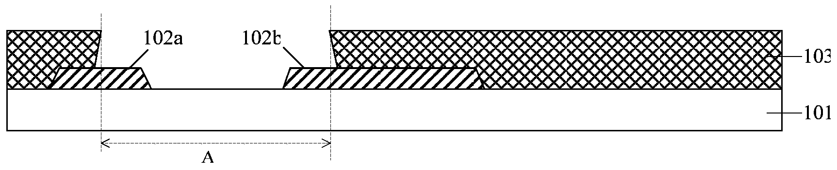
[0051] In step 1, patterns of data lines and source-drain electrode layers are formed on the substrate 101 (transparent substrate, such as a glass substrate or a quartz substrate). Specifically, this step may be to form a source-drain metal thin film on the substrate 101 (which may be formed by sputtering, evaporation or chemical vapor deposition CVD), and then pass a patterning process (usually including photoresist coating, exposure, development, etching, etc.) etching, photoresist stripping, etc.) to form the patterns of the source ...


PUM


Abstract

The invention discloses an array substrate manufacturing method. The array substrate manufacturing method comprises the steps of: forming a pattern including a data line, a source electrode and a drain electrode on a substrate; forming a pattern including an active layer; forming a pattern insulating a grid insulating layer and exposing a region of the drain electrode, which is connected with a to-be-formed anode; forming a pattern including a grid line, a grid electrode and the anode; forming a pattern including a pixel definition layer, an organic material layer and a transparent cathode. The invention also discloses an array substrate and a display device. The array substrate manufacturing method reduces number of times of mask, and therefore saves manufacturing technological process and manufacturing cost.

Description

technical field [0001] The present invention relates to the field of display technology, in particular to an array substrate, a manufacturing method thereof, and a display device. Background technique [0002] Traditional top-emitting AMOLED display devices such as figure 1 As shown, it includes: the first gate 2, the second gate 2' and the gate line (not shown in the figure) formed on the substrate 1, the first gate 2, the second gate 2' and the gate The gate insulating layer 3 above the line, the first active layer 4 and the second active layer 4' formed on the gate insulating layer 3, the first active layer 4 and the second active layer 4' formed on the The etch barrier layer 5, the first source and drain layer 6 (including the first source and the first drain) and the second source and drain layer 6' (including the second source and the first drain) formed on the etch barrier 5 two drains), a passivation layer 7 formed on the first source and drain layer 6 and the seco...

Claims


Application Information

Patent Timeline
Patent Type & Authority Applications(China)
IPC IPC(8): H01L51/56H01L27/32
CPCH01L29/66969H01L29/7869H10K59/12H10K59/1201
Inventor 宋泳锡刘圣烈崔承镇金熙哲
Owner BOE TECH GRP CO LTD
Why Eureka
Try Eureka