Preparation method of metal nanostructure

A kind of metal nanostructure and nanostructure technology, which is applied in the direction of metal material coating process, coating, liquid chemical plating, etc., can solve the lack of precision, roughness and uneven shape of metal nanostructure in controlling the shape and size of metal nanostructures. The uniformity of size and size cannot be guaranteed, so as to achieve the effect of improving light extraction efficiency and light absorption efficiency, simple preparation process and high efficiency

Inactive Publication Date: 2014-03-26
OCEANS KING LIGHTING SCI&TECH CO LTD +2
View PDF1 Cites 26 Cited by
  • Summary
  • Abstract
  • Description
  • Claims
  • Application Information

AI Technical Summary

Problems solved by technology

However, since the preparation process requires the deposition of a thin film first, and the growth of the film has to go through the process of adsorption, nucleation, island formation, and the coarsening and merging of the island, the surface of the thin film (thickness less than 100nm) is relatively rough, so It lacks precision in controlling the shape and size of the metal nanostructure, and the uniformity of the shape and size of the prepared metal nanostructure cannot be guaranteed, which also affects the light extraction efficiency and light absorption efficiency of the metal nanostructure material.

Method used


Image

  • Preparation method of metal nanostructure
  • Preparation method of metal nanostructure
  • Preparation method of metal nanostructure

Examples


Embodiment 1

[0039] A method for preparing a metal nanostructure, comprising the steps of:

[0040] (1) Provide a clean substrate, and make the required nanostructure pattern on the substrate to form a mask, and the part with the pattern on the substrate is transparent to ultraviolet rays;

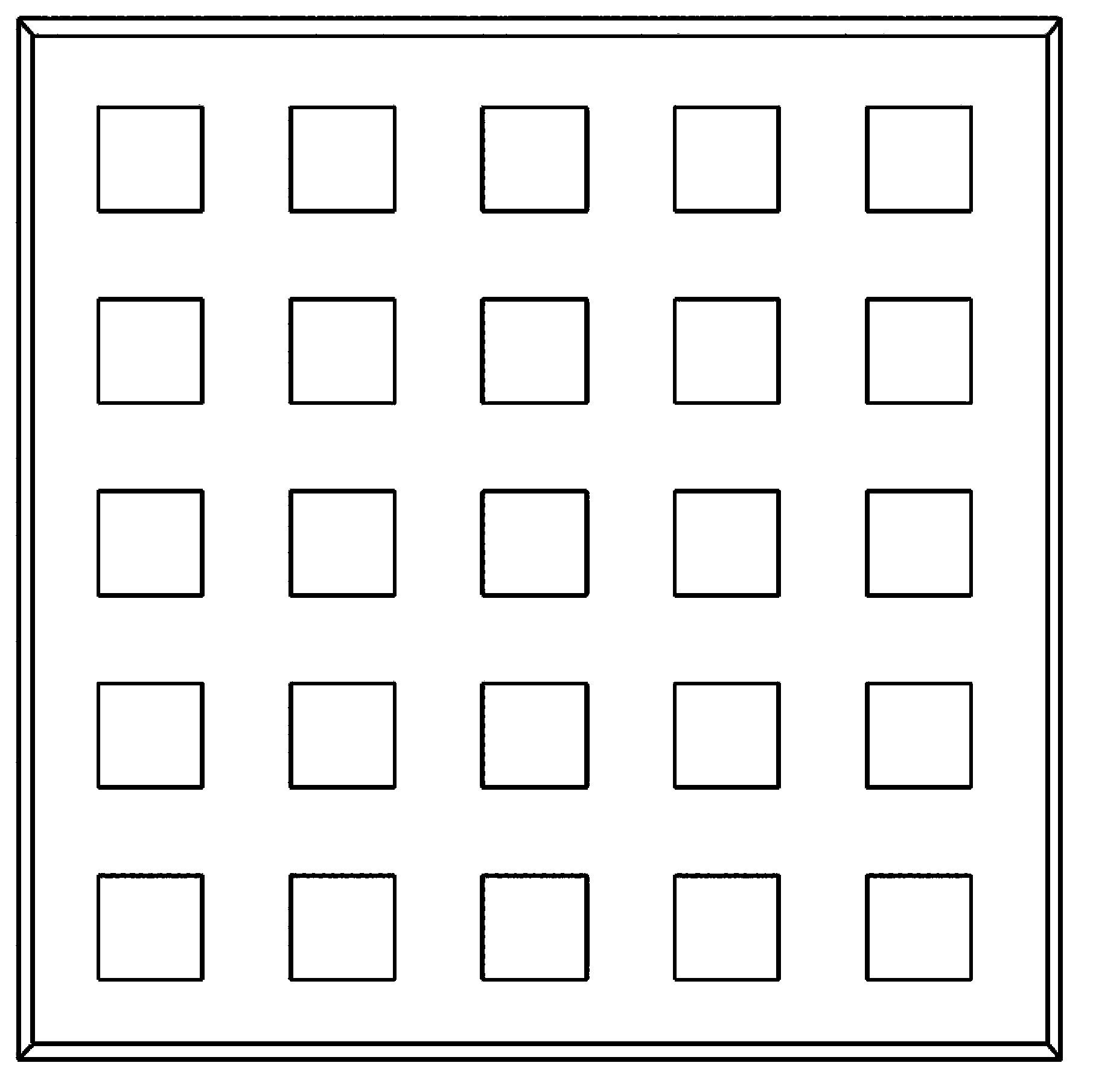
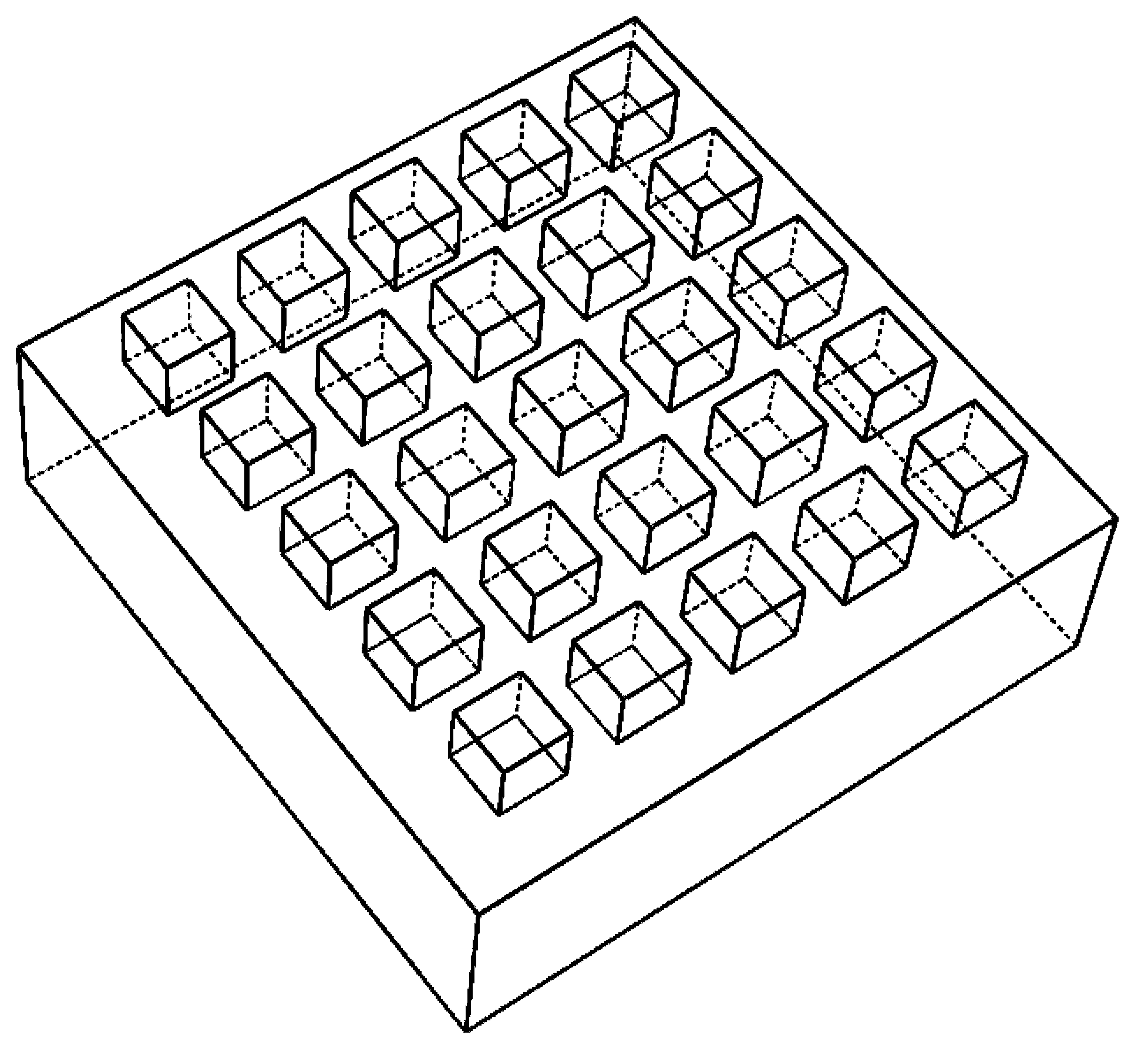
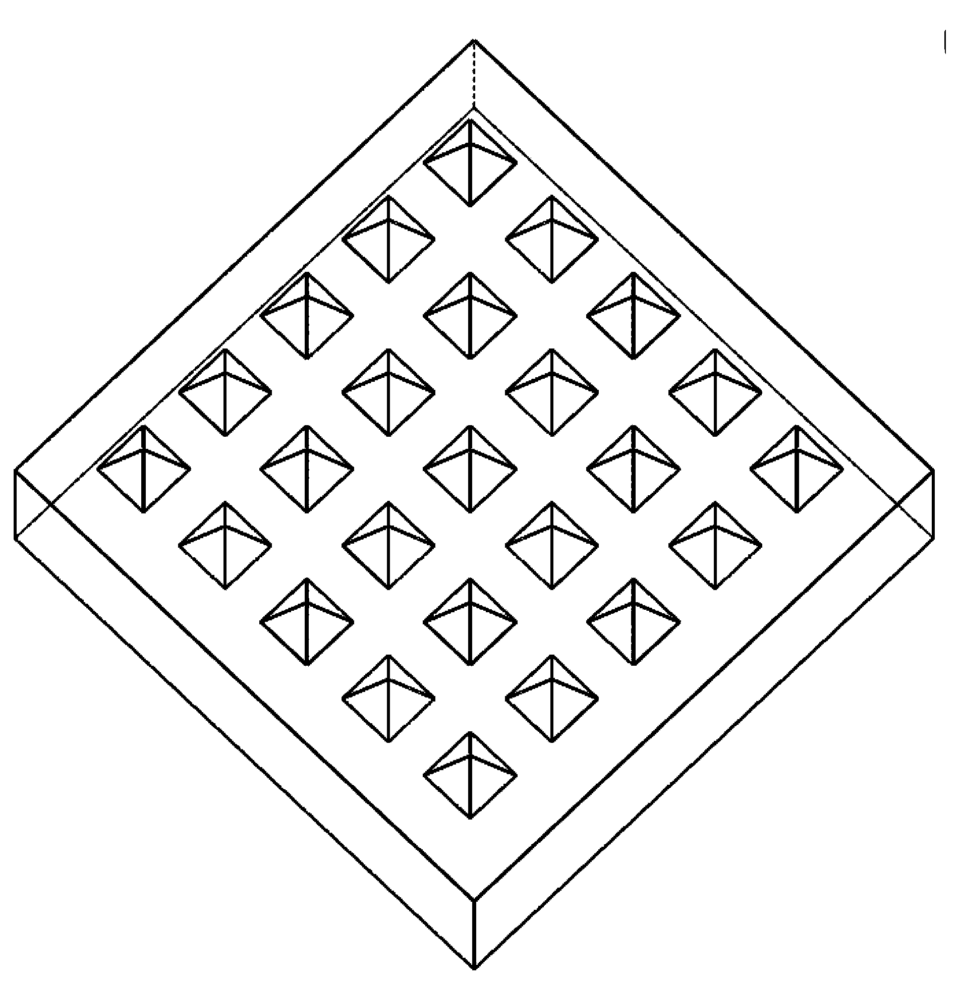
[0041] Select a tungsten steel substrate with a length of 12cm, a width of 12cm, and a thickness of 0.5cm, and clean it; draw a square array pattern with a side length of 40nm and a pitch of 20nm, and import it into a PC connected to an electron beam pattern generator, and control the electron beam through the PC. The beam pattern generator draws the square array pattern in the middle of the substrate at a ratio of 1:1, puts it in an oven and dries it at 60°C for 30 minutes, so that the part with the pattern on the substrate is transparent to ultraviolet light, forming mask board.

[0042](2) Provide a clean and dry substrate, and uniformly coat positive UV photoresist on the substrate, pre-baking, so...

Embodiment 2

[0052] A method for preparing a metal nanostructure, comprising the steps of:

[0053] (1) Provide a clean substrate, and make the required nanostructure pattern on the substrate to form a mask, and the part with the pattern on the substrate is transparent to ultraviolet rays;

[0054] Select an iron oxide substrate with a length of 5cm, a width of 5cm, and a thickness of 0.5cm, and clean it for later use; draw a square array pattern with a side length of 30nm and a spacing of 30nm, and import it into a PC connected to a laser pattern generator, and control it through the PC The laser pattern generator draws the square array pattern to the middle of the substrate at a ratio of 1:1, puts it in an oven and dries it at 80°C for 20 minutes to prepare a mask.

[0055] (2) Provide a clean and dry substrate, and uniformly coat positive UV photoresist on the substrate, pre-baking, so that the positive UV photoresist is cured to form a photoresist substrate;

[0056] Select a gallium ...

Embodiment 3

[0064] A method for preparing a metal nanostructure, comprising the steps of:

[0065] (1) Provide a clean substrate, and make the required nanostructure pattern on the substrate to form a mask, and the part with the pattern on the substrate is transparent to ultraviolet rays;

[0066] Select a chromium substrate with a length of 2cm, a width of 2cm, and a thickness of 0.3cm, and clean it for later use; draw a square array diagram with a side length of 20nm and a spacing of 10nm, and import it into a PC connected to the copying device, and control the copying device through the PC. The square array image is copied to the middle of the chrome substrate at a ratio of 1:2, and placed in an oven to dry at 80°C for 20 minutes, so that the part with the pattern on the substrate is transparent to ultraviolet rays and forms a mask.

[0067] (2) Provide a clean and dry substrate, and uniformly coat positive UV photoresist on the substrate, pre-baking, so that the positive UV photoresis...


PUM

PropertyMeasurementUnit
thicknessaaaaaaaaaa
depthaaaaaaaaaa
thicknessaaaaaaaaaa

Abstract

The invention discloses a preparation method of a metal nanostructure. The preparation method comprises the steps of (1) manufacturing a mask plate; (2) providing a clean and dry base plate, uniformly coating a positive ultraviolet photoresist on the base plate, and pre-baking to ensure that the positive ultraviolet photoresist is solidified to form a photoresist base plate; (3) overlapping the mask plate on the photoresist base plate, and performing exposure, development, residual adhesive removal and hardening under ultraviolet light to obtain a forming mold with shape grooves of a nanostructure graph; (4) depositing a metal in the forming mold by adopting a chemical synthetic method; (5) soaking the forming mold deposited with the metal in an acetone solution, and performing ultrasonic adhesive removal to obtain the metal nanostructure of the nanostructure graph. The preparation method disclosed by the invention is simple in process and high in efficiency; the shape, size and position of the prepared metal nanostructure can be accurately controlled, and the light extraction efficiency and light absorption efficiency of a metal nanostructure material are effectively improved.

Description

technical field [0001] The invention relates to a method for preparing an ultramicrostructure, in particular to a method for preparing a metal nanostructure. Background technique [0002] Metal nanostructured materials have been a research hotspot in the field of optics in recent years. Because their surface plasmons can be excited by light waves to produce very special optical properties, they are widely used in photocatalysis, nano-integrated photonics, optical sensing, biomarkers, medicine, etc. Imaging, solar cells, and surface-enhanced Raman spectroscopy have broad application prospects. [0003] Metal nanostructure materials are generally required to be on the scale of 1-100nm in any dimension of three-dimensional space, and their shape, size, composition, and structure largely determine the performance of metal nanomaterials. Precisely controlling the shape, size, and position of metal nanomaterials is of great significance for using metal nanostructures to excite su...

Claims


Application Information

Patent Timeline
Patent Type & Authority Applications(China)
IPC IPC(8): C23C18/06
Inventor 周明杰王国彪陈贵堂
Owner OCEANS KING LIGHTING SCI&TECH CO LTD
Why Eureka
Try Eureka