Cutting method of lower layer metal wiring

A technology of metal wiring and cutting method, which is applied in the manufacturing of electrical components, electric solid-state devices, semiconductor/solid-state devices, etc., can solve the problems of difficult removal of metal wire redeposition, inability to accurately observe, and incorrectly cut surrounding metal wires, etc. The effect of speeding up the debugging process and failure analysis, improving the efficiency and success rate of line repair

Active Publication Date: 2016-06-08
SHANGHAI HUAHONG GRACE SEMICON MFG CORP
View PDF5 Cites 0 Cited by
  • Summary
  • Abstract
  • Description
  • Claims
  • Application Information

AI Technical Summary

Problems solved by technology

[0003] 1. Due to the influence of the process, the actual shape of the chip will be slightly deviated from the layout (such as the lateral dimension deviation caused by the surface passivation layer), which will lead to a slight deviation in positioning. When the metal wiring is dense, these deviations will cause errors. Cutting Peripheral Wires
[0004] 2. When the depth of a single etching pit reaches more than several microns, there will be problems in the judgment of the etching end point (EPD), whether it is observed by image or current: the deeper the depth of image observation, the weaker the imaging signal, resulting in It cannot be accurately observed, and cannot be used as an accurate EPD; current observation, small etching pits, resulting in weaker incident ion beams per unit area, and deeper depths, resulting in a further decrease in the actual effective area at the bottom of the etching pits, thereby further weakening the ion beam. This eventually results in current observations that are weak, even indistinguishable from noise, and cannot be used as an accurate EPD
[0005] 3. Re-deposition during metal wire etching is not easy to eliminate, resulting in poor cutting effect

Method used


Image

  • Cutting method of lower layer metal wiring
  • Cutting method of lower layer metal wiring
  • Cutting method of lower layer metal wiring

Examples


Embodiment Construction

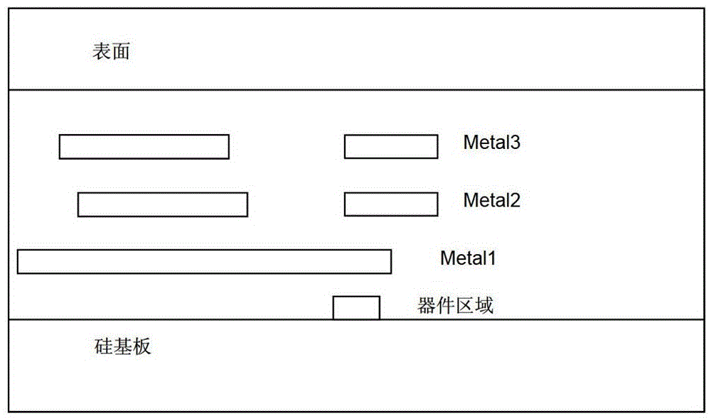
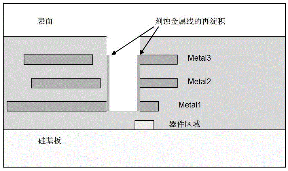
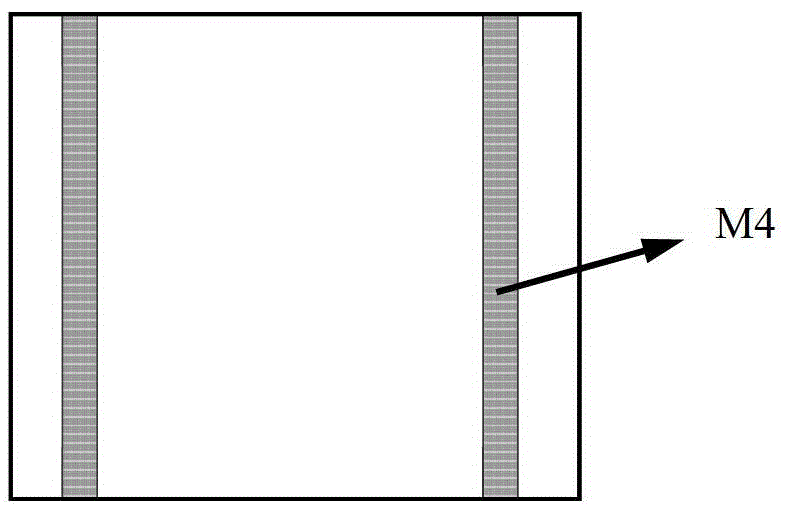
[0024] Focused Ion Beam (FIB): This equipment or technology uses the focused gallium positive ion beam as the incident particle (or primary ion) to hit the surface of the sample, and collects secondary electrons for imaging. Due to the large atomic weight of gallium ions , After acceleration, the kinetic energy is large, so it has a good sputtering etching function, and with a suitable gas system, it can realize auxiliary functions including selective etching and deposition of specific materials. The gas system it is often equipped with is Pt-Dep (platinum metal deposition system), IEE (selective enhanced etching), I-dep (insulating film deposition), etc.; when working, the gas is sprayed on the surface of the sample, and the ion beam bombards When FIB sets the pattern, it not only directly etches the sample surface, but also impacts some gas atoms on the sample surface, and a certain chemical reaction occurs together; by adjusting appropriate parameters, a layer of platinum me...


PUM


Abstract

The invention discloses a safe and precise cutting method for lower metal arranged wire. The safe and precise cutting method comprises the following steps: step one, using a focused ion beam technology according to the following procedures to realize cutting of the lower metal wires: during etching, enabling an IEE (Insulator Enhanced Etching) needle to enter a reaction chamber without opening a valve of the needle, etching under the conditions that the residence time of an iron beam on each pixel is 1 microsecond and the area overlapping proportion is 50%, wherein the size of the outermost etching frame is more than 10mm * 10mm, the size of a new etching frame every time is needed to be at least 10% less than that of the previous frame, the new etching frame does not include metal wires exposed by the previous etching frame, the etching end point is the next layer of exposed metal wires at the position with an interval of more than 1mm with the exposed metal wires so as to expose the metal wires to be cut; step two, cutting the metal wires, etching for 20-50 seconds, and cutting the metal wires; step three, finally cleaning all etching frames through the enhanced etching mode by using a beam current between 500pA and 1000pA. With the adoption of the safe and precise cutting method, the line repair efficiency and success rate of chips are improved, thus, the debugging process during the initial stage of chip design is greatly quickened, the speed of failure analysis is increased, the speed of entering the market of the product is increased, and the mass production yield of chips is increased.

Description

technical field [0001] The invention relates to a circuit repairing technology used in debugging after the initial design and manufacture of a semiconductor chip and chip failure analysis. Background technique [0002] The commonly used cutting method for the lower layer metal wiring is to select a smaller single etching frame after finding the designated cutting point according to the relevant positioning, and then directly etch the metal line from the surface to the designated layer and cut it off. The problems with this method are: [0003] 1. Due to the influence of the process, the actual shape of the chip will be slightly deviated from the layout (such as the lateral dimension deviation caused by the surface passivation layer), which will lead to a slight deviation in positioning. When the metal wiring is dense, these deviations will cause errors. Cut the perimeter wire. [0004] 2. When the depth of a single etching pit reaches more than several microns, there will ...

Claims


Application Information

Patent Timeline
Patent Type & Authority Patents(China)
IPC IPC(8): H01L21/02C23F4/00
CPCH01L21/76894H01L2221/1094
Inventor 赖华平潘永吉
Owner SHANGHAI HUAHONG GRACE SEMICON MFG CORP
Why Eureka
Try Eureka