
Detection method of high resistance of tungsten contact plug

A detection method and tungsten embolism technology, which is applied in measuring devices, semiconductor/solid-state device testing/measurement, instruments, etc., can solve the problems of high resistance of tungsten contact embolism and it is difficult to judge, achieve clear contrast and improve the formation effect

Active Publication Date: 2014-04-02
WUHAN XINXIN SEMICON MFG CO LTD
View PDF4 Cites 11 Cited by
  • Summary
  • Abstract
  • Description
  • Claims
  • Application Information

AI Technical Summary

Problems solved by technology

[0003] The technical problem to be solved by the present invention is to provide a detection method for high resistance of tungsten contact plugs, which solves the technical problem in the prior art that it is difficult to judge the specific cause of high resistance of tungsten contact plugs related to etching

Method used


Image

  • Detection method of high resistance of tungsten contact plug
  • Detection method of high resistance of tungsten contact plug
  • Detection method of high resistance of tungsten contact plug

Examples


Embodiment Construction

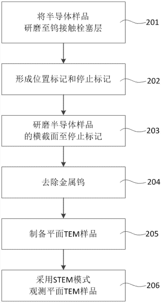
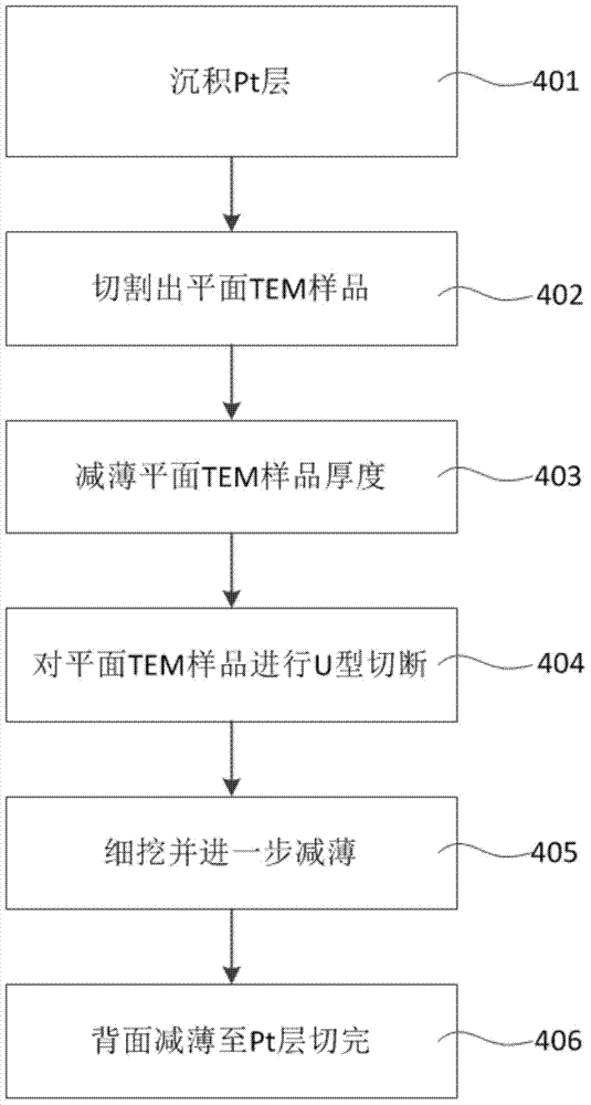
[0028] The principles and features of the present invention are described below in conjunction with the accompanying drawings, and the examples given are only used to explain the present invention, and are not intended to limit the scope of the present invention. In the semiconductor manufacturing industry, there are various inspection equipment, such as transmission electron microscope (TEM), scanning electron microscope (SEM), etc., and scanning transmission electron microscope (STEM) accessories can also be installed on the TEM machine. STEM comprehensively utilizes the principle of scanning and ordinary transmission electron analysis, scans the surface of the sample and penetrates the sample for imaging, which is very suitable for detecting the morphology, size and characteristics of the thin films that make up semiconductor devices. The working principle of STEM is to thin the sample to be tested to about 0.2um by cutting, grinding, ion thinning, etc., and then put it into...


PUM

PropertyMeasurementUnit
Thicknessaaaaaaaaaa
Thicknessaaaaaaaaaa

Abstract

The invention relates to a detection method of high resistance of a tungsten contact plug. The detection method comprises the following steps of grinding a semiconductor sample to a tungsten plug contact layer; forming two location tags used for determining a fail address in an area to be observed of the semiconductor sample, and forming a stop flag on a position, which is close to the fail address; grinding a cross section of the semiconductor sample to the stop flag; digesting the semiconductor sample in boiled hydrogen peroxide until metal tungsten is removed and a cobalt silicide layer is exposed; preparing a planar TEM (Transmission Electron Microscopy) sample; observing the planar TEM sample by adopting STEM (Scan Transmission Electron Microscopy). According to the technical scheme of the invention, the metal tungsten is firstly removed, and then the growth morphology and the quality of the cobalt silicide are observed through a STEM mode, so that the reason for the high resistance of the tungsten contact plug can be quickly found, an improvement direction of a technology is indicated, and the detection method has a very important function of improving formation of the high resistance of the tungsten contact plug.

Description

technical field [0001] The invention relates to the field of semiconductor manufacturing, in particular to a method for detecting high resistance of a tungsten contact plug. Background technique [0002] With the development of semiconductor technology, the integration level of large-scale integrated circuit chips has reached hundreds of millions or even billions of devices. The device is externally connected to the above multi-layer metal through metal silicide and tungsten plug. In the physical failure analysis of two adjacent bits of floating gate or non-flash memory products, the abnormality of tungsten contact plugs is the most suspected object. Leakage or high resistance is the most common cause of abnormal tungsten contact embolism. Usually, electrical failure analysis is performed by measuring the bit cell current to determine whether the cause is leakage or high resistance. In the existing semiconductor manufacturing process, there are mainly two reasons for the f...

Claims


Application Information

Patent Timeline
IPC IPC(8): H01L21/66
CPCG01N23/2202G01N23/2206
Inventor 张顺勇张佐兵高慧敏
Owner WUHAN XINXIN SEMICON MFG CO LTD
Learn More