Structure of fast recovery diode (FRD) and manufacturing method thereof

A technology for recovering diodes and manufacturing methods, applied in the direction of diodes, semiconductor/solid-state device manufacturing, semiconductor devices, etc., can solve problems such as easy degradation, limited implantation depth, and difficult process, so as to improve speed and softness, and improve switching Frequency, the effect of increasing the switching speed

Active Publication Date: 2014-04-02
BYD SEMICON CO LTD
View PDF5 Cites 23 Cited by
  • Summary
  • Abstract
  • Description
  • Claims
  • Application Information

AI Technical Summary

Problems solved by technology

[0004] The devices made by the above-mentioned various methods have obvious defects: although the devices made by electron irradiation can increase the switching frequency of FRD, the switching softness of FRD is reduced at the same time, and the lifetime formed by electron irradiation The control is easy to degrade at high temperature, and this method has limitations on the packaging process conditions; the device made by heavy metal doping, the distribution of heavy metal in the device is uncontrollable; the device made by proton and helium ion implantation, when increasing the operating frequency At the same time, the softness of the switch is also improved, but high-energy ion implantation is required, the cost is high, the process is difficult, and the depth of implantation is limited

Method used


Image

  • Structure of fast recovery diode (FRD) and manufacturing method thereof
  • Structure of fast recovery diode (FRD) and manufacturing method thereof
  • Structure of fast recovery diode (FRD) and manufacturing method thereof

Examples


Embodiment Construction

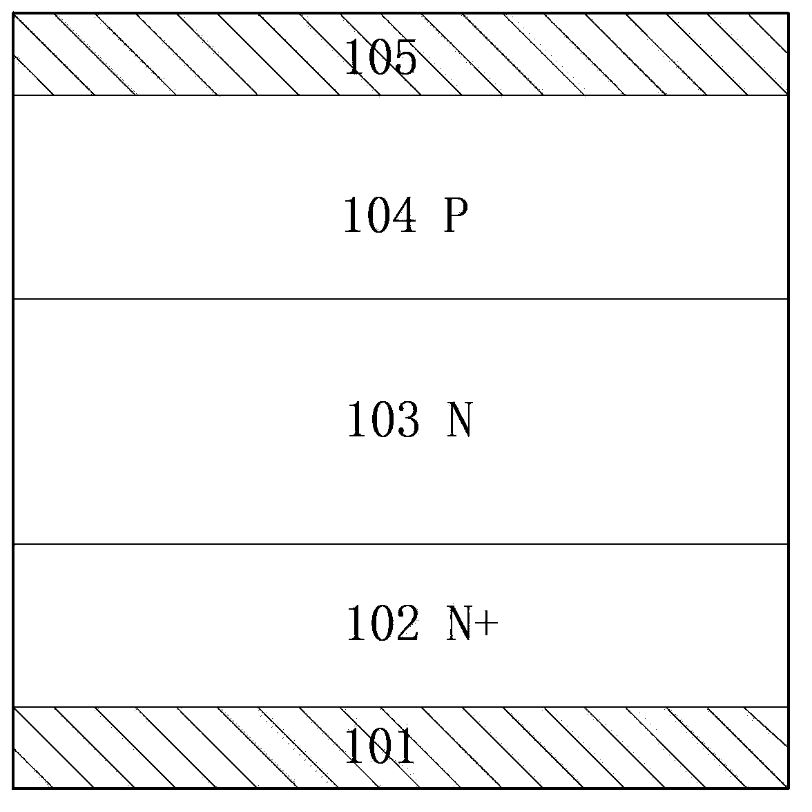
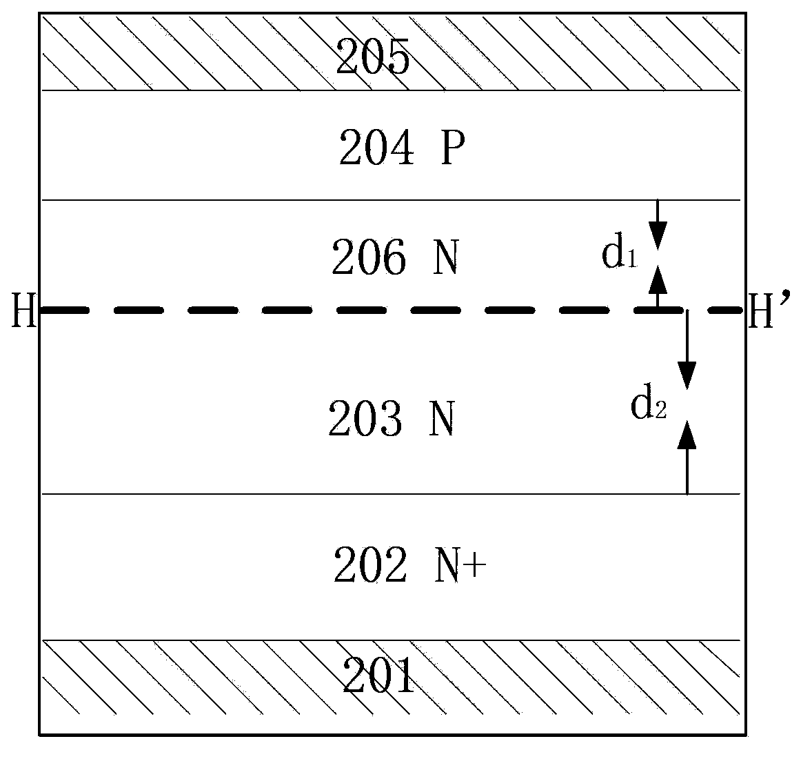
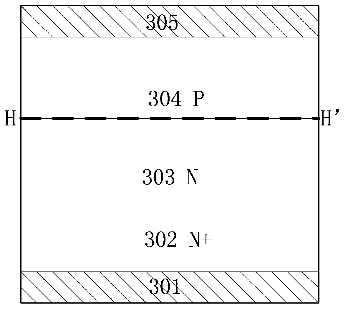
[0032]Embodiments of the present invention are described in detail below, and examples of the embodiments are shown in the accompanying drawings, wherein for the sake of distinction and convenience of expression, the same or components or elements with similar functions are denoted by different symbols in different embodiments . The embodiments described below by referring to the figures are exemplary only for explaining the present invention and should not be construed as limiting the present invention.

[0033] In describing the present invention, it should be understood that the terms "center", "longitudinal", "transverse", "upper", "lower", "front", "rear", "left", "right", " The orientations or positional relationships indicated by "vertical", "horizontal", "top", "bottom", "inner", "outer", etc. are based on the orientation or positional relationships shown in the drawings, and are only for the convenience of describing the present invention and simplifying Describes, b...


PUM


Abstract

The invention provides a structure of a fast recovery diode and a manufacturing method of the fast recovery diode. The structure comprises a cathode metal layer, a cathode area located on the cathode metal layer and comprising a first conduction type, a drift area located on the cathode area and having the first conduction type, an anode area located on the drift area and having a second conduction type, and an anode metal layer located on the anode area, wherein a PN (North Pole) junction is formed at an interface of the drift area and the anode area, and bonding interfaces are formed at the PN junction and / or in a drift area and / or the anode area. The bonding interfaces are introduced, thereby forming a short life area in a fast recovery diode body area, and the position of the bonding interface is precisely controlled to accurately control the life distribution of a carrier in the fast recovery diode body area, and effectively improve the switching speed of the fast recovery diode, and simultaneously ensure the switch softness.

Description

technical field [0001] The invention relates to the field of semiconductor design and manufacture, in particular to a structure of a fast recovery diode and a method thereof. Background technique [0002] FRD (fast recovery diode) has the advantages of high operating frequency and low conduction voltage, and is widely used in power control circuits to play the role of freewheeling or rectifying. With the development of power electronics technology, FRD is required to have higher operating frequency and better switching softness. [0003] figure 1 Shown is a schematic diagram of the structure of a conventional FRD. Taking the FRD of a PIN+ diode as an example, the FRD includes from bottom to top: cathode metal layer 101, cathode layer 102 (N+ region), drift region 103 (N region), anode region 104 (P region) and anode metal layer 105. The operating frequency of the FRD is related to the lifetime of excess carriers stored in the drift region 103 when it is turned off. The s...

Claims


Application Information

Patent Timeline
Patent Type & Authority Applications(China)
IPC IPC(8): H01L29/861H01L29/45H01L21/329H01L29/36
CPCH01L29/06H01L29/0684H01L29/32H01L29/66121H01L29/66204H01L29/868
Inventor 吴海平郝瑞红肖秀光
Owner BYD SEMICON CO LTD
Why Eureka
Try Eureka