CSTBT manufacturing method
A manufacturing method and drift region technology, applied in semiconductor/solid-state device manufacturing, semiconductor devices, electrical components, etc., can solve the problems of increasing process cost and improving process difficulty, and achieve the effect of reducing the difficulty of manufacturing process and reducing manufacturing cost
- Summary
- Abstract
- Description
- Claims
- Application Information
AI Technical Summary
Problems solved by technology
Method used
Image

Examples
Embodiment
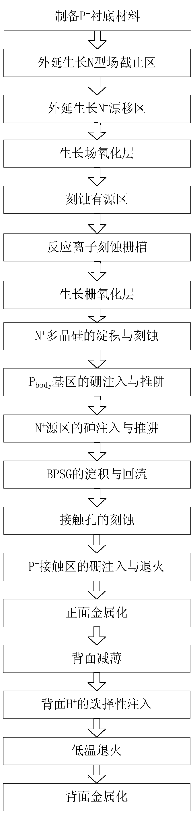
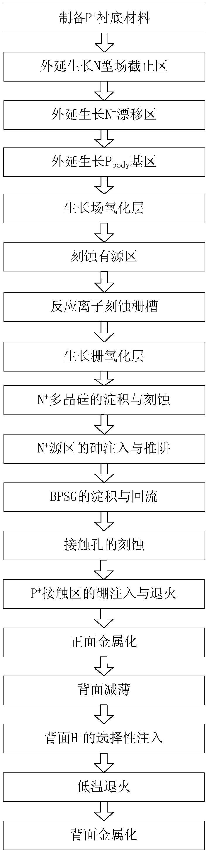
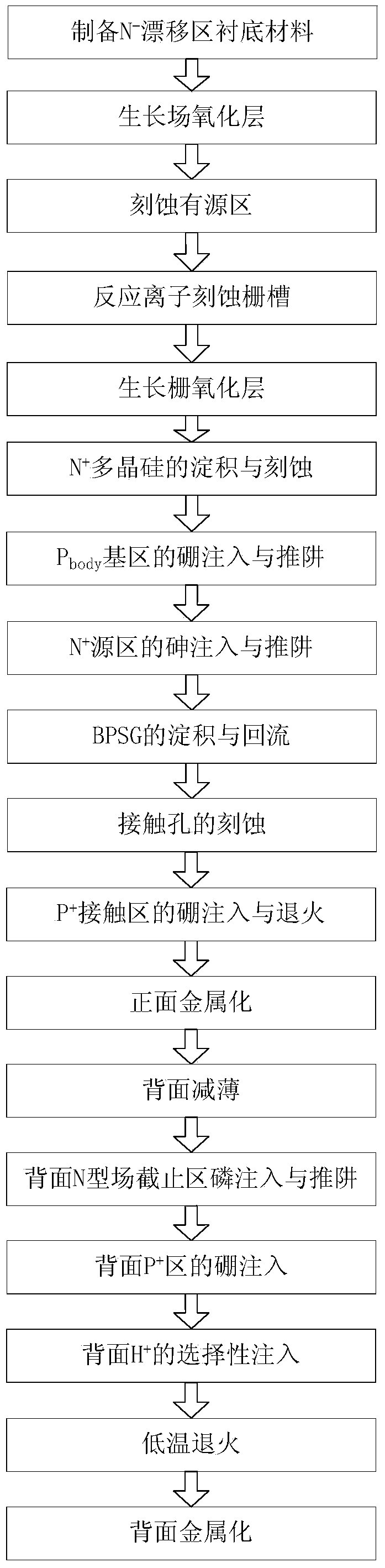
[0126] Taking the manufacturing process of 600V CSTBT as an example, the specific process is as follows:
[0127] (1) Preparation of P + Single crystal silicon wafer 1 substrate material, such as Figure 4 As shown, P + The thickness of the monocrystalline silicon wafer 1 lining is 400-600 μm, the resistivity is 0.0135-0.0375Ω·cm, and the impurity is boron;
[0128] (2) Epitaxial growth of N-type field stop region 2, such as Figure 5 As shown, the thickness of the N-type field stop region 2 is 2 μm, the resistivity is 0.08-0.14 Ω·cm, the growth temperature is 1000-1200° C., and the impurity is phosphorus;
[0129] (3) Epitaxial growth of N - Drift Zone 3, such as Figure 6 Shown, N - The drift region 3 is grown at 1000-1200°C, the impurity is phosphorus, the resistivity is 43.4-86.5Ω·cm, and the thickness is 50μm;
[0130] (4) Growth field oxide layer 4, such as Figure 7 As shown, the growth temperature is 1000-1200 °C, and the thickness is 0.5-1.5 μm;
[0131] (5) Et...
PUM
 Abstract
Description
Claims
Application Information