High-power array light-emitting diode (LED) chip surface radiating structure and manufacturing method

A technology of LED chip and heat dissipation structure, applied in the direction of semiconductor/solid-state device parts, semiconductor devices, electrical components, etc.

Active Publication Date: 2014-04-16
BAOSTEEL METAL
View PDF9 Cites 10 Cited by
  • Summary
  • Abstract
  • Description
  • Claims
  • Application Information

AI Technical Summary

Problems solved by technology

[0004] For the relatively new flip-chip packaging technology at present, because the light is emitted from the surface of sapphire, it effectively avoids the phenomenon that the lead wires block the light, and at the same time most of the heat is emitted from the chip The other side flows into the substrate, which effectively avoids the problem of poor thermal conductivity of the sapphire substrate, so that the heat dissipation effect and electro-optical conversion efficiency are significantly improved, but when the chip power is large, there will also be poor heat dissipation.
In the nitride array LED chip, the distance between adjacent light-emitting units is only 10-30 microns. Considering the problem of inclination during photolithography, the distance will be smaller, which will cause the heat generated by the light-emitting units to be unable to dissipate well. The luminous efficiency of the light-emitting unit will be greatly reduced with the increase of the chip temperature. If the distance between the light-emitting units is simply increased, the effective light-emitting area will be reduced.
The problem of heat dissipation is an urgent problem to be solved for high-power array LEDs. If this problem is not effectively solved, the application of nitride array LED chips will be greatly restricted.

Method used


Image

  • High-power array light-emitting diode (LED) chip surface radiating structure and manufacturing method
  • High-power array light-emitting diode (LED) chip surface radiating structure and manufacturing method
  • High-power array light-emitting diode (LED) chip surface radiating structure and manufacturing method

Examples


Embodiment Construction

[0056] The present invention will be further described below with reference to the embodiments and accompanying drawings.

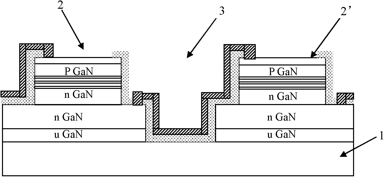
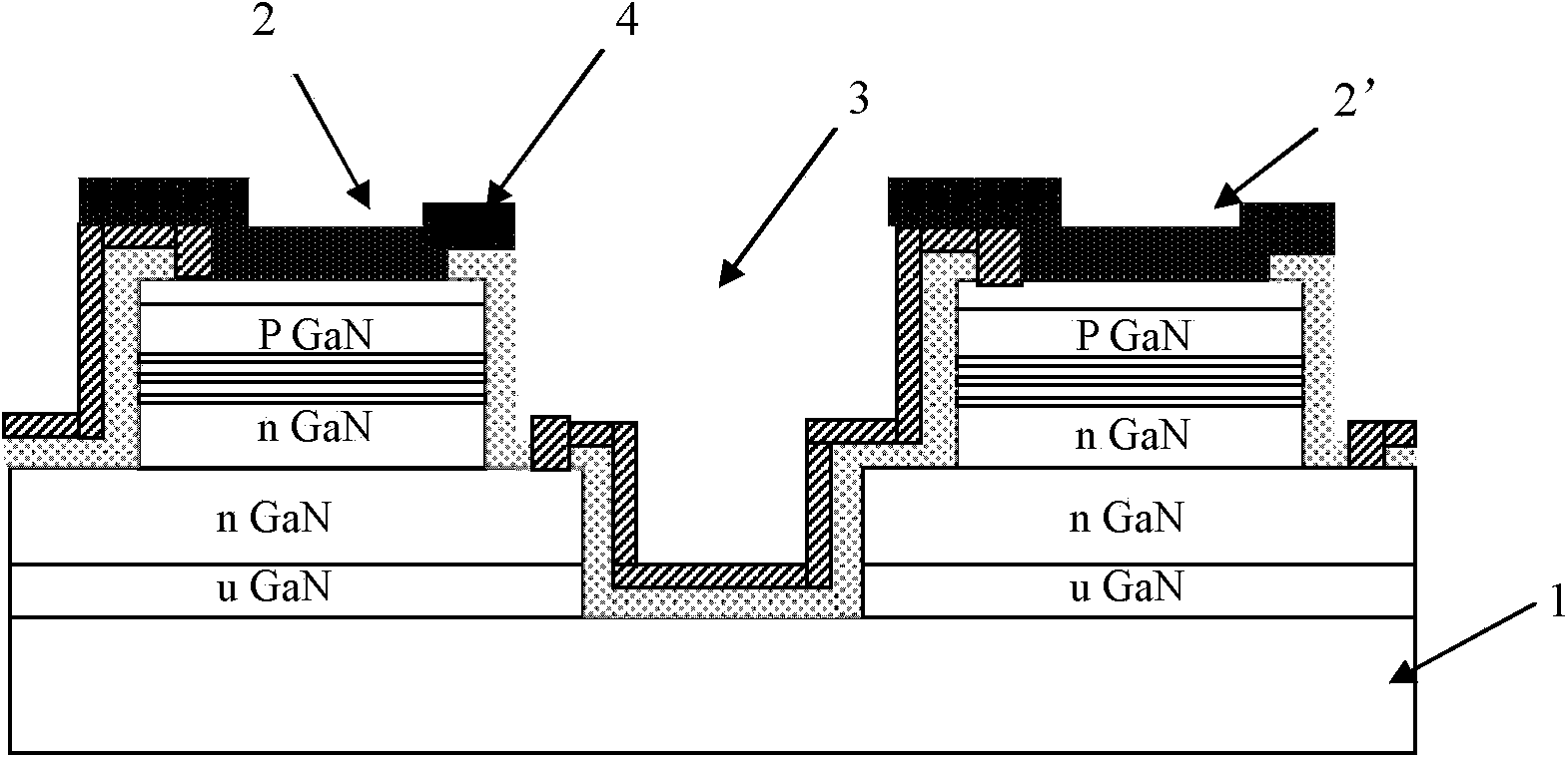
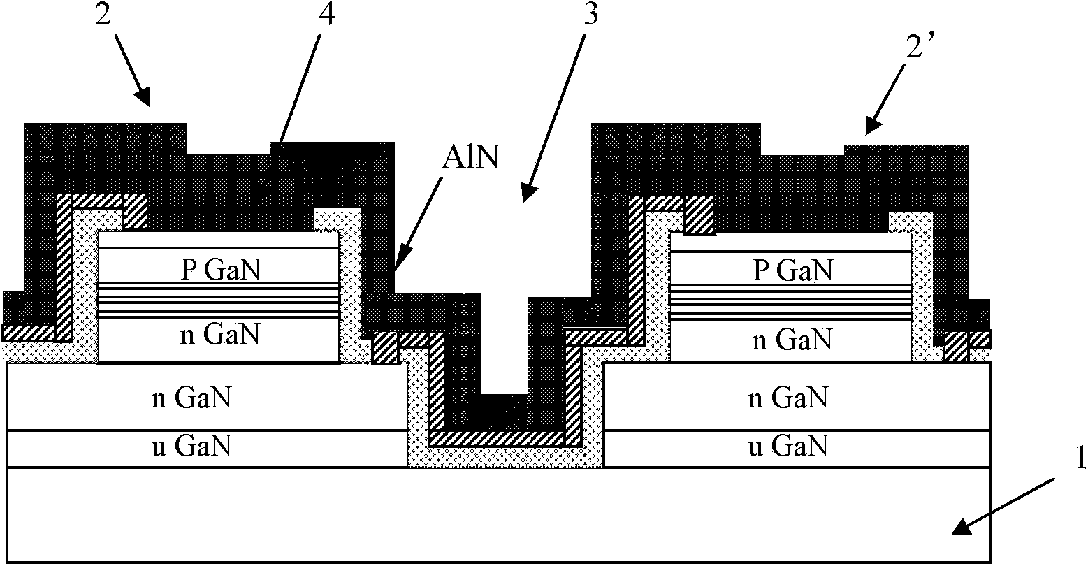
[0057] see Figure 13 , the cross-sectional view of the surface heat dissipation structure of the high-power array LED chip of the present invention, the substrate 1 is the most common sapphire substrate, the distance between the adjacent light-emitting units 2 and 2' is 10-30 microns, and the light-emitting units 2 and 2' are connected by bridges. The metal is connected. Although the isolation trench 3 between the light-emitting units 2 and 2' is filled with a silicon dioxide layer and a titanium / aluminum / titanium / gold bridge layer, the trench still has a certain depth. Easy to hide bubbles. When the light-emitting unit emits light, a large amount of heat will be generated, and this part of the heat will diffuse in all directions. The thermal conductivity of sapphire is poor. If this part of the heat is not properly handled, the temperature of the light...


PUM


Abstract

Provided are a high-power array light-emitting diode (LED) chip surface radiating structure and a manufacturing method thereof. An aluminum nitride layer and a copper layer are sequentially deposited in an isolation groove between light-emitting units of the array LED chip from bottom to top to form a grid metal layer, namely a heat sink channel used for guiding out the heat produced by the light-emitting units of the chip is formed between the light-emitting units of the chip. The structure and the method can effectively improve the radiating performance. The process is simple and easy to achieve, the radiating structure is suitable for laboratory research and development and batch production, the technical difficulty of the existing high-power array LED chip radiating can be effectively solved, and the structure and the method are of great significance in achievement of high-power LED lighting.

Description

technical field [0001] The invention relates to the technical field of LEDs, in particular to a high-power array LED chip surface heat dissipation structure and a manufacturing method. Background technique [0002] At present, the operating voltage of ordinary DC nitride LEDs on the market does not exceed 5V, and our daily electricity consumption is usually 110V-240V, which is extremely inconvenient to use. The emergence of nitride array LED effectively solves the above problems. The array LED chip refers to the integration of LED light-emitting units on the substrate through a certain arrangement, so that each light-emitting unit bears a certain voltage division, and the purpose of using under high voltage can be achieved by adjusting the number of light-emitting units. The conversion efficiency is greatly improved. Ordinary low-power LEDs have limited their application in daily lighting due to their low operating voltage. Nitride array LEDs can be directly connected to A...

Claims


Application Information

Patent Timeline
Patent Type & Authority Applications(China)
IPC IPC(8): H01L23/367H01L23/31H01L23/373
CPCH01L24/24H01L2924/12041H01L2224/24H01L2924/00H01L2924/00012
Inventor 吴维群贾砚林于得鲁陈阿平熊峰曹清卢金雄胡勇
Owner BAOSTEEL METAL
Why Eureka
Try Eureka