Method for controlling cooling of wafer in semiconductor process

A technology for controlling wafers and semiconductors, applied in semiconductor/solid-state device manufacturing, electrical components, circuits, etc., can solve problems such as adjusting cooling conditions, excessive nitrogen consumption, and low cooling efficiency, and achieve nitrogen resource conservation, control and shortening, The effect of increasing productivity

Active Publication Date: 2014-04-23
BEIJING SEVENSTAR ELECTRONICS CO LTD
View PDF5 Cites 8 Cited by
  • Summary
  • Abstract
  • Description
  • Claims
  • Application Information

AI Technical Summary

Problems solved by technology

The aforementioned existing wafer cooling methods do not adjust the cooling conditions for various parameters that affect the cooling time for different processes of oxidation, LPCVD and low-temperature annealing, but use the same fixed cooling conditions
The disadvantage of this cooling method is that, on the one hand, during the cooling process, when the oxygen content reaches the control target, the set nitrogen flow rate and cooling wind speed will not change, resulting in excessive nitrogen consumption, especially for the oxidation process, which is harmful to the wafer. The oxygen content requirement in the load-bearing area is not high, which increases the consumption of nitrogen; on the other hand, the cooling conditions are not adjusted reasonably according to the characteristics of various parameters that affect the cooling time, resulting in the length of the cooling time cannot be grasped, and the Uncontrolled, its actual cooling efficiency is low, which adversely affects wafer throughput

Method used


Image

  • Method for controlling cooling of wafer in semiconductor process

Examples


Embodiment 1

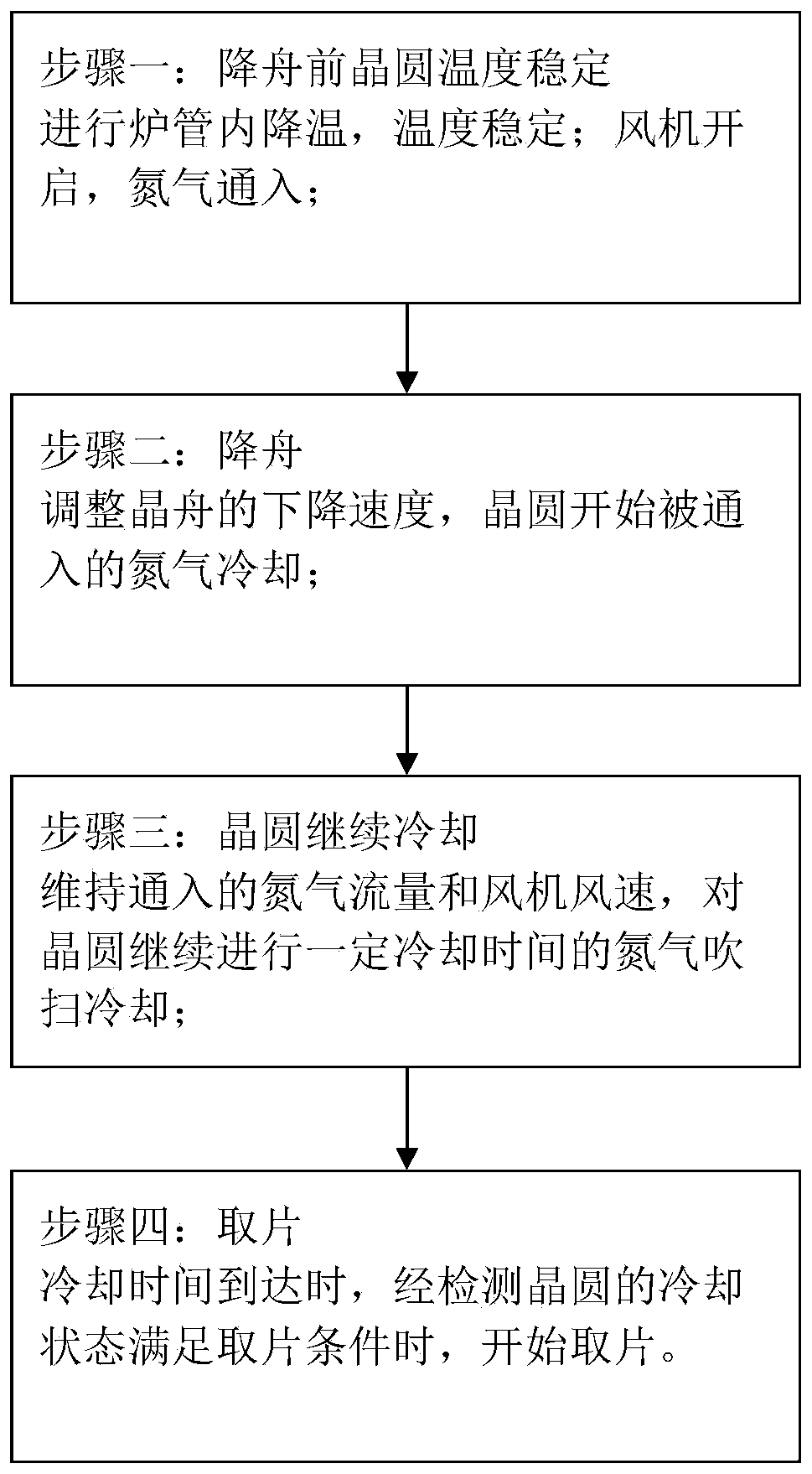
[0032] In this example, see figure 1 . figure 1 It is a flowchart of a method for controlling wafer cooling in a semiconductor process of the present invention. As shown in the figure, the method for controlling wafer cooling of the present invention is aimed at oxidation, low-pressure chemical vapor deposition or The low-temperature annealing process is implemented, including four steps of stabilizing the wafer temperature before lowering the boat, lowering the boat, continuing to cool the wafer, and picking up the wafer, as follows:

[0033] Step 1: The temperature of the wafer is stabilized before landing the boat. In the cooling stage of the furnace tube of the semiconductor process, according to the different types of processes, the temperature in the furnace tube is lowered to a temperature range of different heights and stabilized; and, according to the different requirements for oxygen content of different types of processes, the vertical The flow of nitrogen gas use...

Embodiment 2

[0054] In this embodiment, for the oxidation process, the following relevant cooling control parameters are set and implemented:

[0055] (1) The temperature of the wafer is stabilized before the boat is lowered: before the boat is lowered, the temperature is stabilized, and the temperature in the furnace tube is lowered to 600°C to stabilize; the number of wafers in a batch is 125, and the size of the wafer is 300mm;

[0056] (2) The fan is turned on: the wind speed is 0.3m / s, which can form a relatively stable laminar airflow;

[0057] (3) For the vertical furnace oxidation process, the requirements for the oxygen content in the load-bearing area are not high, and air is introduced into the load-bearing area instead of nitrogen for purging and cooling. The air flow rate is 300slm; 200mm / min;

[0058] (4) Continue cooling of the wafer: under nitrogen purge, the cooling time of the wafer in the loading area is 25 minutes, and the temperature of the wafer has reached below 50°...

Embodiment 3

[0061] In this embodiment, for the low-pressure chemical vapor deposition process, the following relevant cooling control parameters are set and implemented:

[0062] (1) The temperature of the wafer is stabilized before the boat is lowered: before the boat is lowered, the temperature is stabilized, the temperature in the furnace tube is lowered to 500°C to stabilize, and the pressure is returned to normal pressure; the number of wafers in a batch is 125 pieces, and the specifications of the wafer The size is 300mm;

[0063] (2) The fan is turned on: the wind speed is 0.4m / s, which can form a relatively stable laminar airflow;

[0064] (3) For the vertical furnace low-pressure chemical vapor deposition process, the oxygen content in the load-bearing area is required to be relatively high, requiring <5ppm, and the flow rate of nitrogen gas is 800slm, which not only ensures the cooling effect of the wafer, but also ensures the oxygen content in the load-bearing area. The conten...


PUM


Abstract

The invention discloses a method for controlling cooling of a wafer in a semiconductor process. Aiming at different processes of oxidation, low-pressure chemical vapor deposition or low-temperature annealing, an unloading speed of a wafer boat is regulated according to a temperature before the boat is unloaded; simultaneously, according to different requirements of different processes on oxygen content, a cooling wind speed is regulated, nitrogen flow is controlled in high and low different ranges and in the unloading process, the wafer is sufficiently cooled and then is taken out in a bearing region. According to the invention, the cooling control parameters such as a wafer precooling temperature, the unloading speed, the nitrogen flow, the cooling wind speed and the like are optimized and combined to be utilized, so that the oxygen content is controlled to reach the standard, effective control on cooling of the wafer in the unloading stage of the process is implemented, the temperature of the wafer can be rapidly and effectively reduced and cooling time is controlled and shortened, therefore, wafer capacity is improved and nitrogen resources used as cooling media are obviously reduced.

Description

technical field [0001] The invention relates to a method for cooling a wafer in a vertical furnace equipment used for semiconductor integrated circuit processing, and more specifically, to a method for using targeted control means according to different semiconductor processes, opposing A method for cooling wafers in the boat drop stage of the furnace equipment process. Background technique [0002] With the development of semiconductor integrated circuit manufacturing technology, the feature size is continuously reduced, which makes the integration of chips higher and higher, and puts forward higher requirements for integrated circuit manufacturing and process equipment. The latest process development is increasingly subject to process equipment. restrict. In terms of vertical furnace equipment, in order to ensure the realization of the above process and material properties, the heat treatment process puts forward higher requirements for the indicators of vertical furnace ...

Claims


Application Information

Patent Timeline
Patent Type & Authority Applications(China)
IPC IPC(8): H01L21/02H01L21/67
CPCH01L21/67011
Inventor 林伟华王兵兰天宋辰龙
Owner BEIJING SEVENSTAR ELECTRONICS CO LTD
Why Eureka
Try Eureka